Semiconductor device
a semiconductor device and semiconductor technology, applied in semiconductor devices, semiconductor/solid-state device details, lighting and heating apparatus, etc., can solve the problems of increasing pressure loss, difficult miniaturization of semiconductor devices, and difficult reducing the size of base plates, so as to minimize the size of semiconductor devices and improve the workability of jackets.
- Summary
- Abstract
- Description
- Claims
- Application Information
AI Technical Summary
Benefits of technology
Problems solved by technology
Method used
Image

Examples
first preferred embodiment
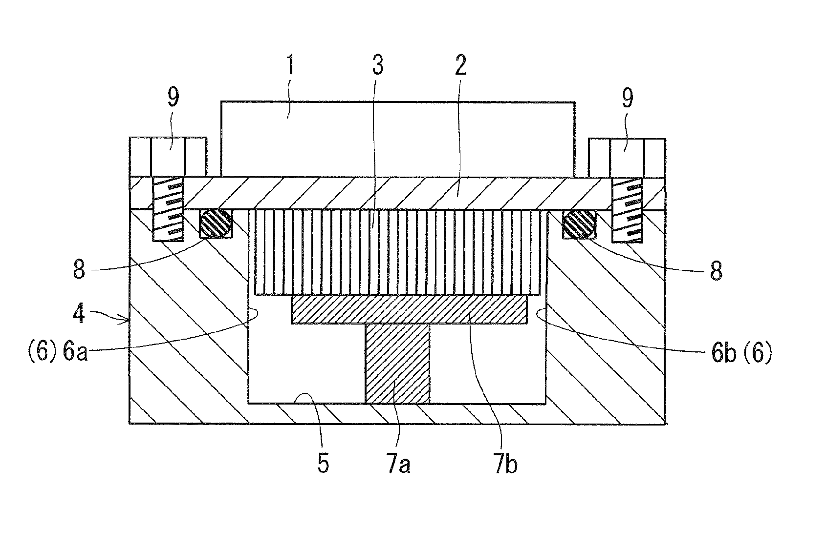
[0029]A first preferred embodiment of the present invention will be described below with reference to the drawings. FIG. 1 is a schematic cross sectional view of a semiconductor device according to the first preferred embodiment. The semiconductor device includes a semiconductor element 1, a base plate 2, cooling fins 3, a jacket 4, and a header partition wall 7. The semiconductor element 1 is, for example, a wide band gap semiconductor element and mounted on an upper surface of the base plate 2.
[0030]The plurality of cooling fins 3 are disposed on the lower surface of the base plate 2. More specifically, the plurality of cooling fins 3 are disposed, on the lower surface of the base plate 2, in a region corresponding to a region where the semiconductor element 1 mounted on the upper surface of the base plate 2 is disposed. The cooling fins 3 are disposed with a predetermined space therebetween such that they protrude downward from the lower surface of the base plate 2. The cooling f...
second preferred embodiment
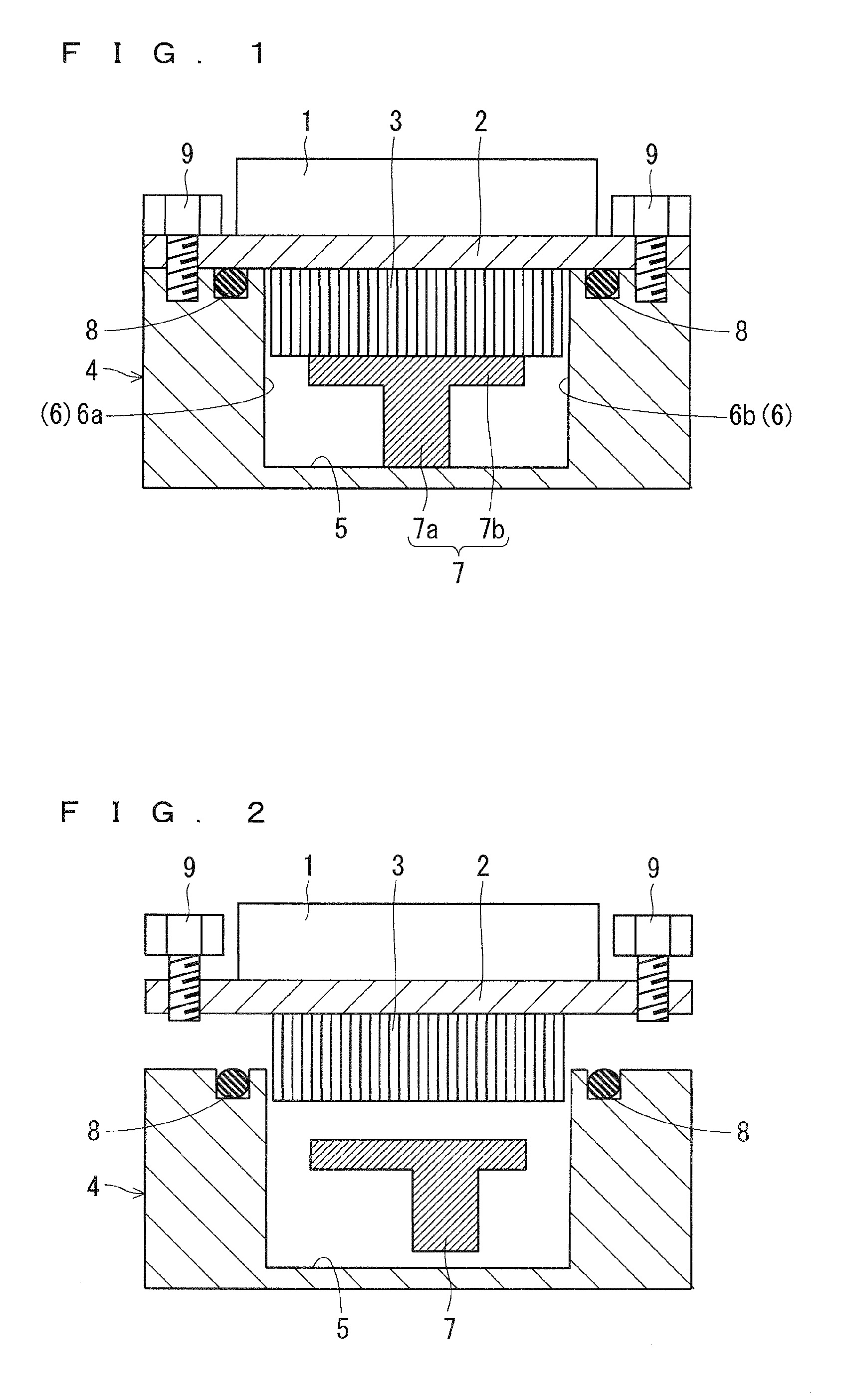
[0047]Next, a semiconductor device according to a second preferred embodiment will be described. FIG. 4 is a schematic cross sectional view showing a state during assembling in the semiconductor device according to the second preferred embodiment. In the second preferred embodiment, the same components as those described in the first preferred embodiment are denoted by the same references, which are not described here.
[0048]In the second preferred embodiment, the header partition wall 7 is formed so as to be dividable into a plurality of pieces. For example, as shown in FIG. 4, the header partition wall 7 has a structure that divides pieces vertically into two. More specifically, in the header partition wall 7, the vertical partition wall 7a and the horizontal partition wall 7b are formed so as to be dividable. The vertical partition wall 7a and the horizontal partition wall 7b are assembled by bolts, for example.
[0049]Next, a modification of the second preferred embodiment will be ...
third preferred embodiment
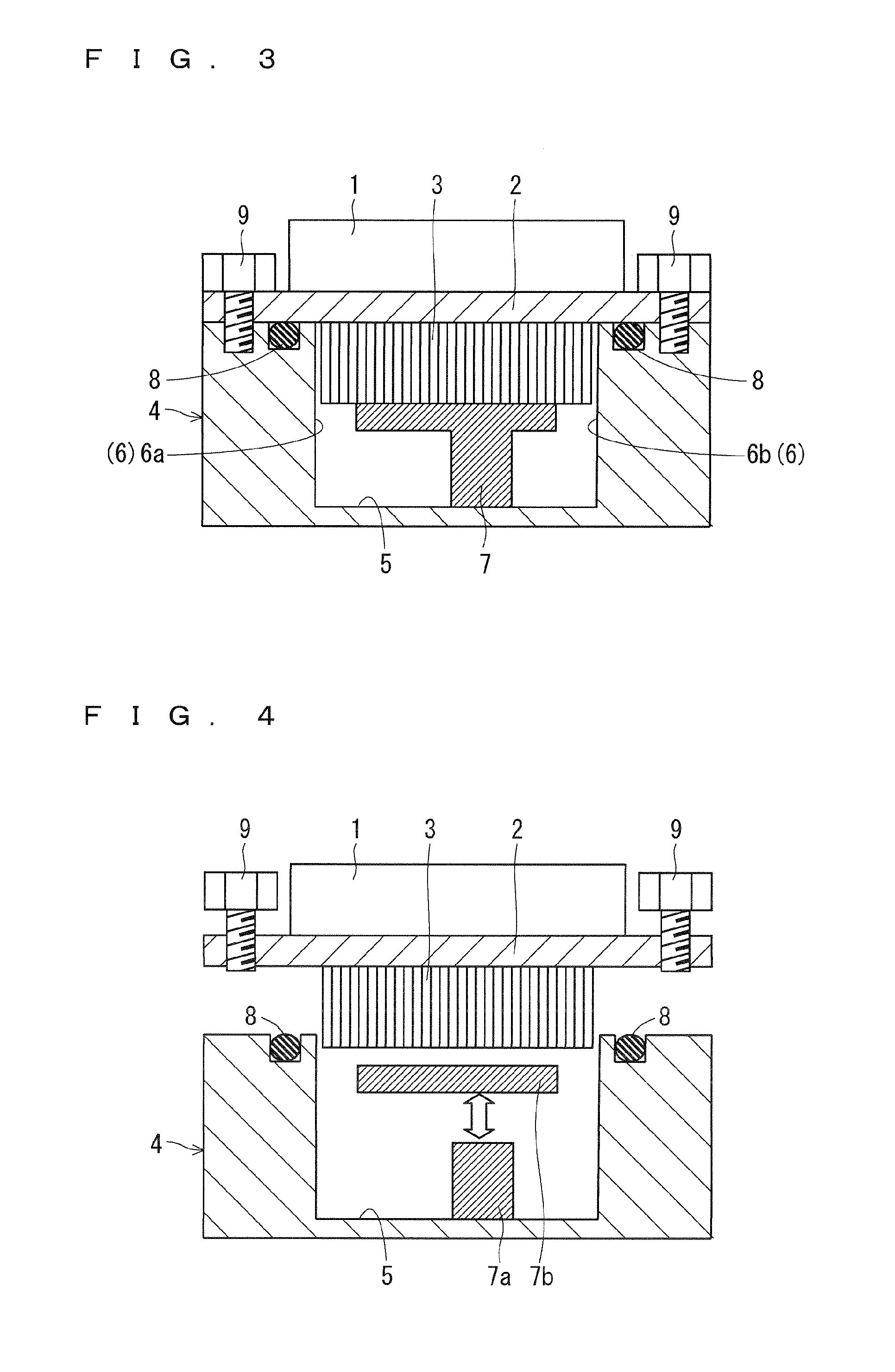
[0054]Next, a semiconductor device according to the third preferred embodiment will be described. FIG. 8 is a schematic cross sectional view of the semiconductor device according to the third preferred embodiment. In the third preferred embodiment, the same components as those described in the first and the second preferred embodiments are denoted by the same references, which are not described here.
[0055]In the third preferred embodiment, as shown in FIG. 8, the outflow-side opening 6b is formed to be smaller than the inflow-side opening 6a. More specifically, as described above, the inflow-side opening 6a and the outflow-side opening 6b are formed with the inner wall of the jacket 4 and the header partition wall 7. A distance between the inner wall of the header 5 (inner wall on left side in FIG. 8) and one of the side surfaces of the horizontal partition wall 7b (left side surface in FIG. 8) is longer than a distance between the inner wall of the header 5 (inner wall on right sid...
PUM
 Abstract
Description
Claims
Application Information
 - R&D Engineer
- R&D Manager
- IP Professional
- Industry Leading Data Capabilities
- Powerful AI technology
- Patent DNA Extraction
Browse by: Latest US Patents, China's latest patents, Technical Efficacy Thesaurus, Application Domain, Technology Topic.
© 2024 PatSnap. All rights reserved.Legal|Privacy policy|Modern Slavery Act Transparency Statement|Sitemap