Organic el display device

a display device and electroluminescent technology, applied in the direction of thermoelectric device junction materials, semiconductor devices, electrical apparatus, etc., can solve the problems of increasing the pixel pitch, affecting the quality of the image, and the contact hole 32/b>, etc., to achieve the effect of suppressing shading, high opening ratio of a pixel, and high quality imag

Active Publication Date: 2015-04-02
JAPAN DISPLAY INC
View PDF5 Cites 26 Cited by
  • Summary
  • Abstract
  • Description
  • Claims
  • Application Information

AI Technical Summary

Benefits of technology

[0015]The present invention aims at providing an organic EL display device that suppresses shading, and obtains a high quality image while maintaining a high opening ratio of a pixel.

Problems solved by technology

This leads to such a problem that the formation of the contact hole 32 is disadvantageous in the high definition of the organic EL display device.
As a result, an useless non-emitting area becomes large.
An increase in the pixel pitch is disadvantageous in higher definition, and the increase in the pixel pitch is caused by an increase in the width of the bank 12, which means an increase in the non-emitting area.

Method used


Image

  • Organic el display device
  • Organic el display device
  • Organic el display device

Examples


first embodiment

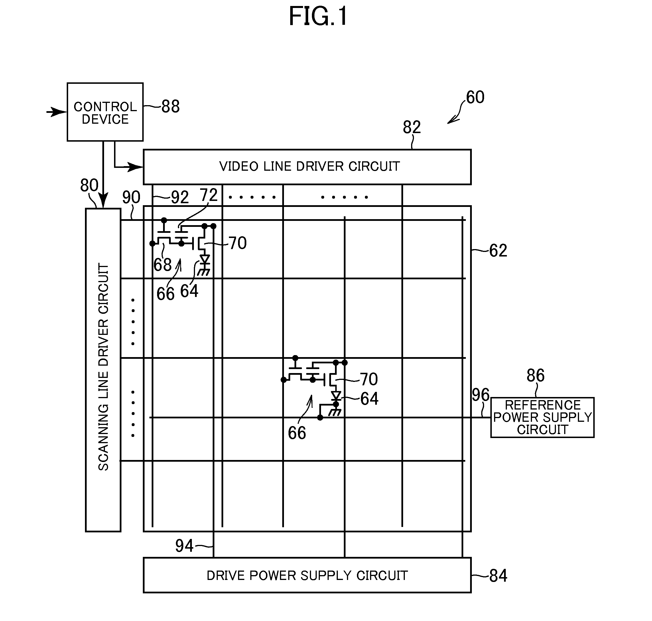
[0030]An organic EL display device is an active matrix display device, and is incorporated into a television, a personal computer, a mobile terminal, and a cellular phone as a display panel. FIG. 1 is a schematic view illustrating a general configuration of an organic EL display device 60 according to a first embodiment of the present invention. The organic EL display device 60 includes a pixel array portion 62 which is a display area for displaying an image, and a drive portion that drives the pixel array portion 62.

[0031]In the pixel array portion 62, OLEDs 64 and pixel circuits 66 are arranged in a matrix in correspondence with pixels (or sub-pixels). Each of the pixel circuits 66 includes plural thin film transistors (TFT) 68, 70, and a capacitor 72. An anode electrode of each OLED 64 is connected to the drive TFT 70. Also, cathode electrodes of all the OLEDs 64 are configured by a common electrode as will be described later.

[0032]On the other hand, the drive portion includes a ...

second embodiment

[0064]A description will be given of the organic EL display device 60 according to a second embodiment of the present invention below. In this embodiment, the components common to those in the first embodiment are denoted by identical symbols, and a description of those components will be basically omitted, and differences from the first embodiment will be mainly described.

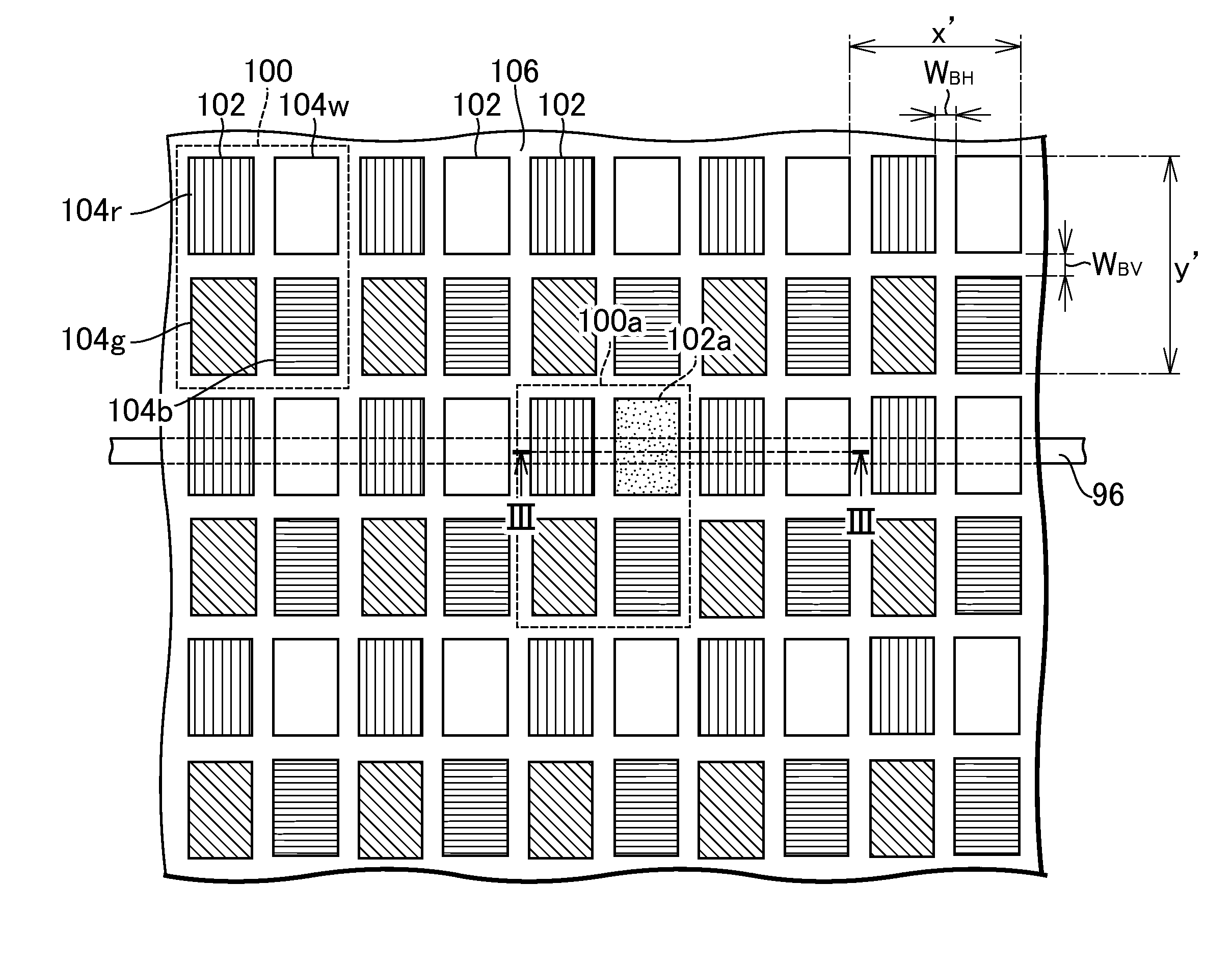
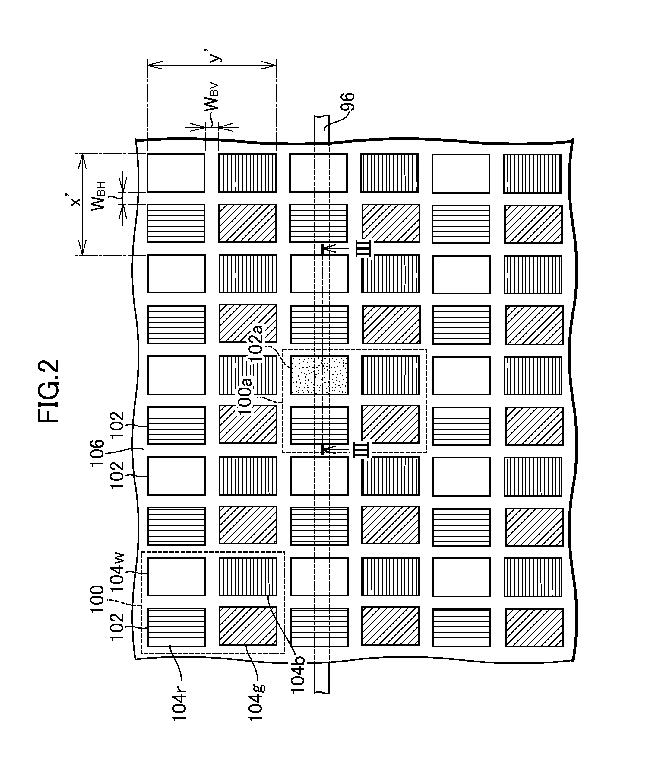
[0065]Each of the pixels 100 according the second embodiment includes four sub-pixels of RGBW which are Bayer-arrayed as in the first embodiment. Differences between the second embodiment and the first embodiment reside in the structure of the irregular pixel. FIG. 5 is a schematic plan view of an irregular pixel 100b according to the second embodiment. In the irregular pixel 100b, the cathode contact 126 is formed in a part of an area 160 corresponding to an opening area of the W sub-pixel 104w of each basic pixel 100 instead of the structure of the organic light emitting element. Specifically, the area 160 is pa...

third embodiment

[0067]A description will be given of the organic EL display device 60 according a third embodiment of the present invention. In this embodiment, the components common to those in the first embodiment are denoted by identical symbols, and a description of those components will be basically omitted, and differences from the first embodiment will be mainly described.

[0068]FIG. 6 is a schematic partial plan view of a pixel array portion 62 in an organic EL display device 60 according to this embodiment. This embodiment is different from the first embodiment in that a basic pixel 200 includes three sub-pixels of RGB, and the cathode contact 126 is formed in an opening area 102b located at a position in an irregular pixel 200a corresponding to the B sub-pixel in the basic pixel 200.

[0069]In this embodiment, the irregular pixel 200a includes two sub-pixels of RG. For that reason, a deficit of the B sub-pixel caused by the provision of the cathode contact 126 cannot be compensated by signal...


PUM


Abstract

In an organic EL display device, a resistance of a cathode electrode of OLEDs is substantially reduced while maintaining a higher opening ratio of pixels as an entire display area. A reference power supply line is formed on a glass substrate, and receives a reference potential for driving the OLED. The OLED is formed on the glass substrate where the reference power supply line is formed, and has a structure in which a lower electrode, an organic material layer, and an upper electrode that is a cathode electrode common to plural pixels are laminated on each other in the order from the bottom. In some of the plural pixels, a cathode contact that penetrates through the organic material layer, and electrically connects the upper electrode to the reference power supply line is formed within an opening area corresponding to a W sub-pixel.

Description

CROSS-REFERENCE TO RELATED APPLICATION[0001]The present application claims priority from Japanese application JP2013-202935 filed on Sep. 30, 2013, the content of which is hereby incorporated by reference into this application.BACKGROUND OF THE INVENTION[0002]1. Field of the Invention[0003]The present invention relates to an organic electroluminescent (EL) display device, and more particularly to homogenization of a potential of an electrode common to plural pixels arrayed in a display area among electrodes of organic light emitting elements.[0004]2. Description of the Prior Art(s)[0005]The organic EL display device has a structure in which a TFT substrate is bonded to a counter substrate. FIG. 7 is a schematically partial cross-sectional view of a display area of a TFT substrate 4 in a related art organic EL display device 2, which illustrates a vertical cross-section along a horizontal direction of the display area. The TFT substrate 4 is configured, for example, so that a circuit...

Claims


Application Information

Patent Timeline
Patent Type & Authority Applications(United States)
IPC IPC(8): H01L27/32
CPCH01L27/3241H01L27/3213H10K59/351H10K59/38H10K59/122H10K59/131H10K50/824H10K2102/3026H10K59/123H10K59/1216
Inventor OOOKA, HIROSHISAKAMOTO, HIROTSUGUSATO, TOSHIHIRO
Owner JAPAN DISPLAY INC
Why Eureka
Try Eureka