Peeling Method and Light-Emitting Device

a technology of light-emitting devices and peeling processes, which is applied in the direction of thermoelectric devices, chemistry apparatuses and processes, and other domestic objects, can solve the problems of high stress applied to functional elements and functional elements broken in some cases, so as to improve the yield of a peeling process, and improve the yield of a fabrication process

Active Publication Date: 2015-05-07
SEMICON ENERGY LAB CO LTD
View PDF3 Cites 41 Cited by
  • Summary
  • Abstract
  • Description
  • Claims
  • Application Information

AI Technical Summary

Benefits of technology

[0019]One embodiment of the present invention can improve the yield of a peeling process. One embodiment of the present invention can improve the yield of a fabrication process of a semiconductor device, a light-emitting device, a display device, an electronic appliance, or a lighting device. In particular, one embodiment of the present invention can improve the yield of a fabrication process of a semicon

Problems solved by technology

When it is difficult to perform peeling at a peeling interface in a peeling step, high st

Method used


Image

  • Peeling Method and Light-Emitting Device
  • Peeling Method and Light-Emitting Device
  • Peeling Method and Light-Emitting Device

Examples


embodiment 1

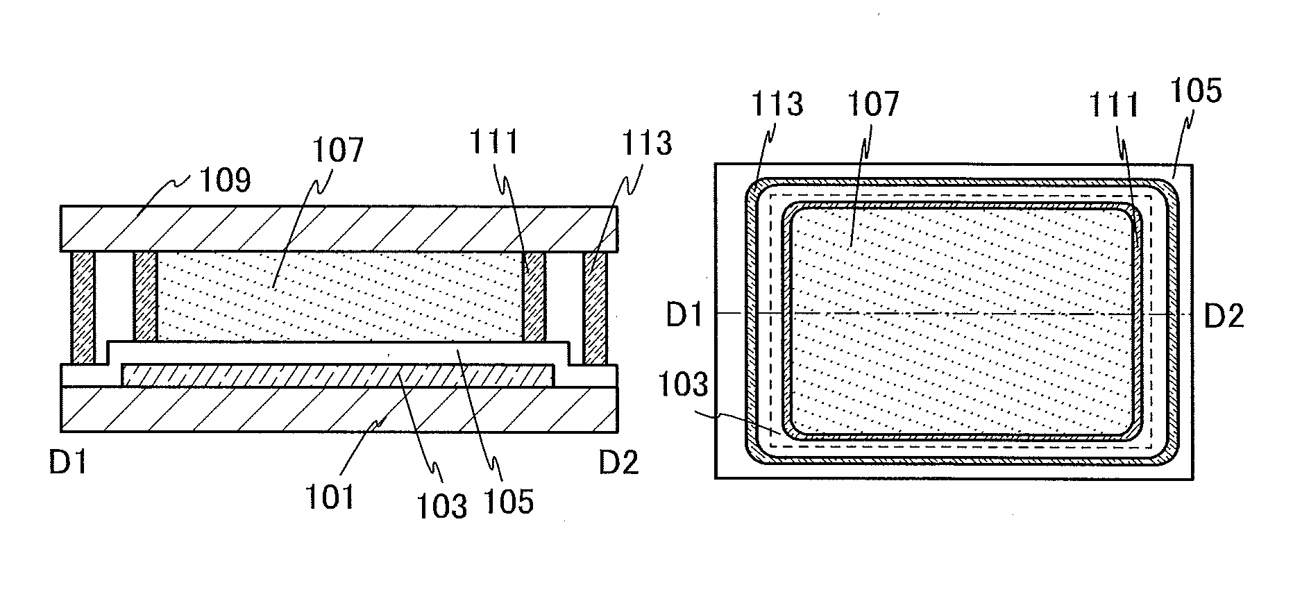
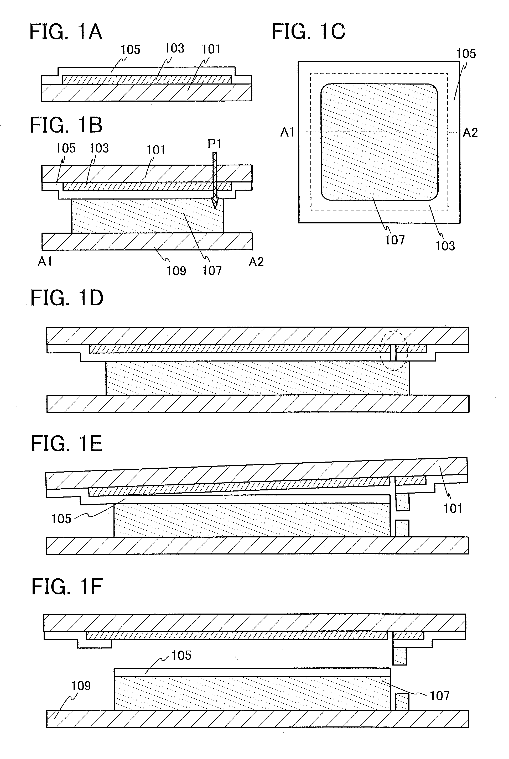
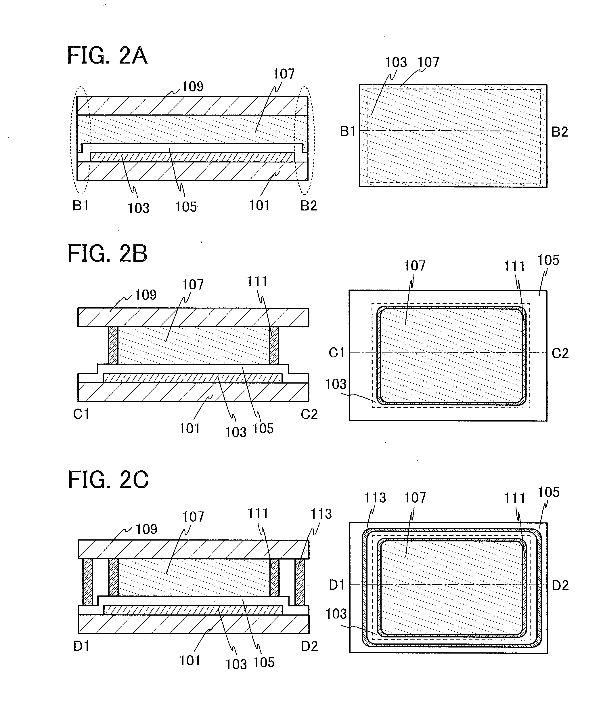
[0063]In this embodiment, a peeling method of one embodiment of the present invention is described with reference to FIGS. 1A to 1F, FIGS. 2A to 2C, FIGS. 3A to 3D, FIGS. 4A to 4D, FIGS. 5A to 5D, FIGS. 6A to 6D, FIGS. 7A to 7D, FIGS. 8A to 8C, and FIGS. 9A to 9I.

[0064]The peeling method of one embodiment of the present invention includes a first step of forming a peeling layer to a thickness of, for example, greater than or equal to 0.1 nm and less than 10 nm over a substrate, a second step of forming, on the peeling layer, a layer to be peeled including a first layer in contact with the peeling layer, a third step of separating parts of the peeling layer and parts of the first layer to form a peeling trigger, and a fourth step of separating the peeling layer and the layer to be peeled.

[0065]When the layer to be peeled has high tensile stress in the separation of the peeling layer and the layer to be peeled, the layer to be peeled is cracked or film breakage is caused in some cases...

embodiment 2

[0164]In this embodiment, a flexible light-emitting device that can be fabricated according to one embodiment of the present invention is described with reference to FIGS. 10A to 10C, FIGS. 11A to 11C, FIGS. 12A1, 12A2, 12B, and 12C, FIGS. 13A and 13B, and FIGS. 14A1, 14A2, 14B, and 14C.

[0165]FIGS. 10A to 10C, FIGS. 11A to 11C, FIGS. 12A1, 12A2, 12B, and 12C, FIGS. 13A and 13B, and FIGS. 14A1, 14A2, 14B, and 14C illustrate examples of flexible light-emitting devices each including an organic EL element as a light-emitting element. The flexible light-emitting devices of embodiments of the present invention can be bent with a radius of curvature of greater than or equal to 1 mm and less than or equal to 150 mm. The direction in which the light-emitting device is bent is not limited. The number of bent portions may be one or more than one. For example, the light-emitting device can be folded in two or three.

[0166]A light-emitting device of one embodiment of the present invention includ...

structure example 1

[0169]FIG. 10A is a plan view of a light-emitting device, and FIGS. 10B and 10C are each an example of a cross-sectional view taken along the dashed-dotted line X1-Y1 in FIG. 10A. The light-emitting devices illustrated in FIGS. 10A to 10C are bottom-emission light-emitting devices.

[0170]The light-emitting devices in FIGS. 10B and 10C each include a flexible substrate 419, an adhesive layer 422, an insulating layer 424, a conductive layer 406, a conductive layer 416, an insulating layer 405, an organic EL element 450 (a first electrode 401, an EL layer 402, and a second electrode 403), a bonding layer 407, and a flexible substrate 428. The first electrode 401, the insulating layer 424, the adhesive layer 422, and the flexible substrate 419 transmit visible light.

[0171]The organic EL element 450 is provided over the flexible substrate 419 with the adhesive layer 422 and the insulating layer 424 therebetween. The organic EL element 450 is sealed by the flexible substrate 419, the bondi...


PUM

PropertyMeasurementUnit
Thicknessaaaaaaaaaa
Thicknessaaaaaaaaaa
Nanoscale particle sizeaaaaaaaaaa

Abstract

The yield of a peeling process is improved. A first step of forming a peeling layer to a thickness of greater than or equal to 0.1 nm and less than 10 nm over a substrate; a second step of forming, on the peeling layer, a layer to be peeled including a first layer in contact with the peeling layer; a third step of separating parts of the peeling layer and parts of the first layer to form a peeling trigger; and a fourth step of separating the peeling layer and the layer to be peeled are performed. The use of the thin peeling layer can improve the yield of a peeling process regardless of the structure of the layer to be peeled.

Description

BACKGROUND OF THE INVENTION[0001]1. Field of the Invention[0002]The present invention relates to an object, a method, or a fabrication method. In addition, the present invention relates to a process, a machine, manufacture, or a composition of matter. One embodiment of the present invention relates to a semiconductor device, a light-emitting device, a display device, an electronic appliance, a lighting device, and a method for fabricating these devices. In particular, one embodiment of the present invention relates to a light-emitting device using an organic electroluminescence (hereinafter also referred to as EL) phenomenon, and a method for fabricating the light-emitting device. In particular, one embodiment of the present invention relates to a peeling method and a method for fabricating a device including a peeling process.[0003]2. Description of the Related Art[0004]In recent years, a flexible device in which a functional element such as a semiconductor element, a display eleme...

Claims


Application Information

Patent Timeline
IPC IPC(8): B32B43/00H01L51/00H01L51/52H01L21/311
CPCB32B43/006H01L21/31105B32B2457/00H01L51/524H01L51/0097B32B2309/105B32B2315/08Y10T156/11Y10T156/1184Y10T156/1978Y10T156/1168Y10T156/1142Y10T156/1967H10K59/12H10K71/80H10K77/111H10K50/85H10K50/84H10K2102/311H01L2221/68386B32B38/10H01L21/68757
Inventor YASUMOTO, SEIJISATO, MASATAKAAOYAMA, TOMOYAKOMATSU, RYU
Owner SEMICON ENERGY LAB CO LTD
Why Eureka
Try Eureka