Trimming silicon fin width through oxidation and etch

a technology of oxidation and etching, which is applied in the direction of basic electric elements, electrical apparatus, semiconductor devices, etc., can solve the problems of reducing critical dimensions and difficult fabrication of high aspect ratio finfets, and achieve the effect of reducing the width of the mandrel structur

Inactive Publication Date: 2015-05-21
APPLIED MATERIALS INC
View PDF11 Cites 15 Cited by
  • Summary
  • Abstract
  • Description
  • Claims
  • Application Information

AI Technical Summary

Benefits of technology

[0008]In one embodiment, a method of forming a fin structure on a substrate is provided. The method comprises etching a silicon layer to form a trench defining a mandrel structure and oxidizing sidewalls of the mandrel structure and a bottom surface of the trench to form an oxidized surface. The oxidized surface is etched to reduce a width of the mandrel structure and an insulator material is deposited over the silicon layer. The mandrel structure is then etched and a semiconducting material is formed on the mandrel structure. Finally, a portion of the insulator material and the semiconducting material are planarized.
[0009]In another embodiment, a method of forming a fin structure on a substrate is provided. The method comprises etching a silicon layer to form a trench defining a silicon mandrel structure and oxidizing sidewalls of the mandrel structure and a bottom surface of the trench to form an oxidized surface. The oxidized surface comprises silicon dioxide and has a thickness of between about 2 nm and about 5 nm. The silicon dioxide is etched to reduce a width of the silicon mandrel structure to between about 5 nm and about 8 nm and an oxide material is deposited over the silicon layer. The silicon mandrel structure is then etched and a semiconducting material is formed on the silicon mandrel structure. Finally, a portion of the oxide material and the semiconducting material are planarized.
[0010]In yet another embodiment, a method of forming a fin structure on a substrate is provided. The method comprises de

Problems solved by technology

Fabrication of high aspect ratio FinFETs is difficult as a result of the reduced critical dimensions required for sub-10 nm nodes.

Method used


Image

  • Trimming silicon fin width through oxidation and etch
  • Trimming silicon fin width through oxidation and etch
  • Trimming silicon fin width through oxidation and etch

Examples


Embodiment Construction

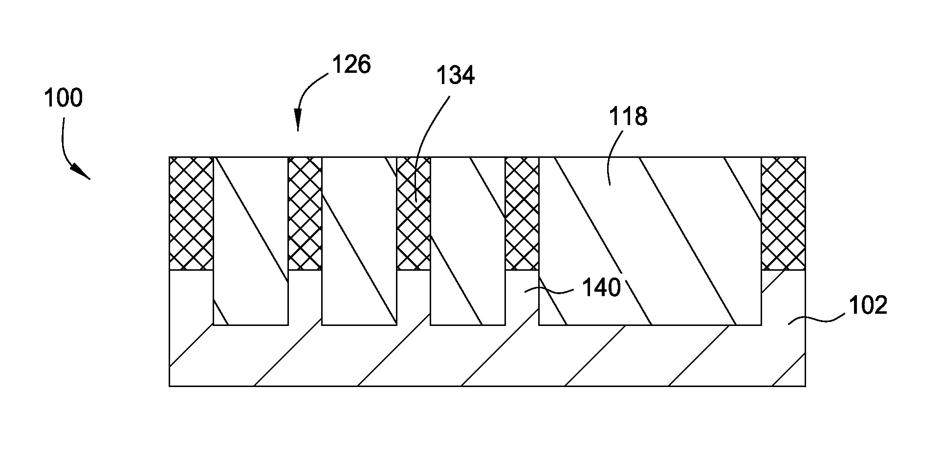
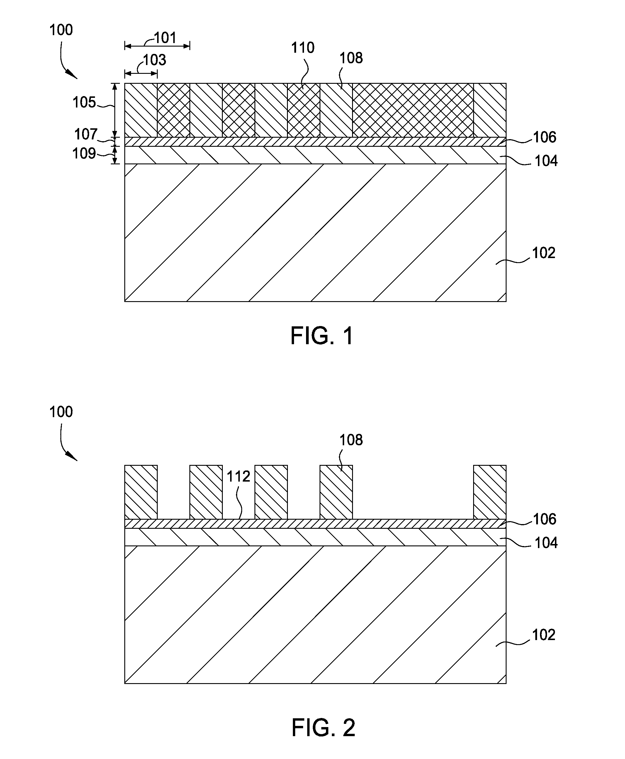
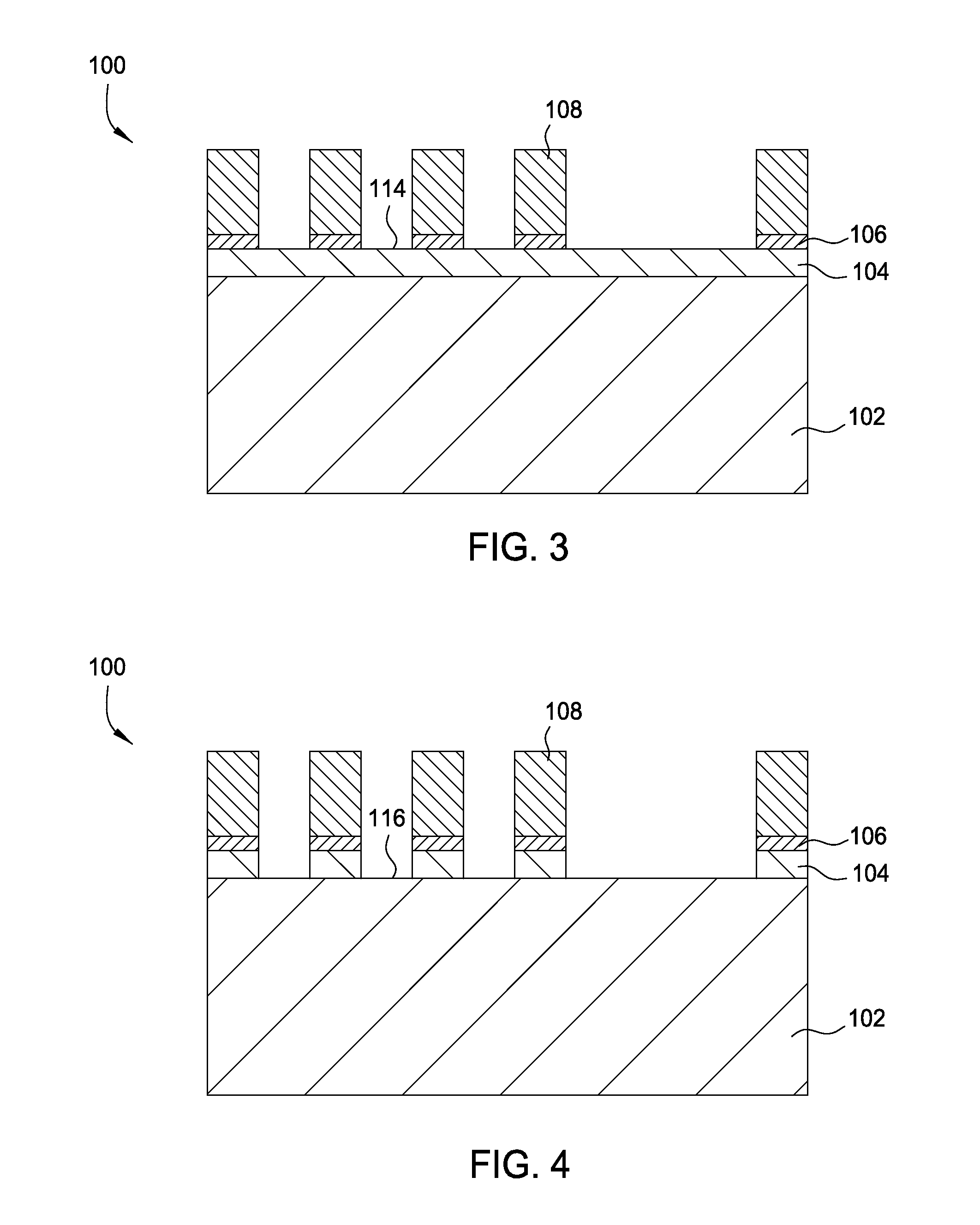
[0034]Embodiments described herein generally relate to methods of forming features for microelectronic devices. More specifically, embodiments described herein generally relate to methods of forming sub-10 nm node FinFETs. Various processing steps are performed on a substrate to provide a trench defining a mandrel structure. Sidewalls of the mandrel structure and a bottom surface of the trench are oxidized and subsequently etched to reduce a width of the mandrel structure. The oxidation and etching of the mandrel structure may be repeated until a desired width of the mandrel structure is achieved. A semiconducting material is subsequently deposited on a regrowth region of the mandrel structure to form a fin structure. Oxidizing and etching the mandrel structure provides a method for forming the fin structure which can achieve sub-10 nm node dimensions and provide increasingly smaller FinFETs.

[0035]FIG. 1 is a cross-sectional view of a substrate 100 having various layers formed there...


PUM


Abstract

Embodiments described herein generally relate to methods of forming sub-10 nm node FinFETs. Various processing steps are performed on a substrate to provide a trench defining a mandrel structure. Sidewalls of the mandrel structure and a bottom surface of the trench are oxidized and subsequently etched to reduce a width of the mandrel structure. The oxidation and etching of the mandrel structure may be repeated until a desired width of the mandrel structure is achieved. A semiconducting material is subsequently deposited on a regrowth region of the mandrel structure to form a fin structure. The oxidizing and etching the mandrel structure provides a method for forming the fin structure which can achieve sub-10 nm node dimensions and provide increasingly smaller FinFETs.

Description

CROSS-REFERENCE TO RELATED APPLICATIONS[0001]This application claims benefit to U.S. Provisional Patent Application Ser. No. 61 / 906,249, filed Nov. 19, 2013, and U.S. Provisional Patent Application Ser. No. 61 / 906,623, filed Nov. 20, 2013, both of which are incorporated herein by reference in their entirety.BACKGROUND[0002]1. Field[0003]Embodiments described herein generally relate to processes for forming silicon fins in a FinFET structure. More specifically, embodiments described herein relate to trimming silicon fin width through oxidation and etch.[0004]2. Description of the Related Art[0005]In response to an increased need for smaller electronic devices with denser circuits, devices with three dimensional (3D) structures have been developed. An example of such devices may include FinFETs having conductive fin-like structures that are raised vertically above a horizontally extending substrate. Conventional FinFETs may be formed on a substrate, such as a semiconducting substrate ...

Claims


Application Information

Patent Timeline
IPC IPC(8): H01L21/02H01L21/306
CPCH01L21/02587H01L21/02532H01L21/02658H01L21/30604H01L21/02126H01L21/02236H01L21/02252H01L21/02255H01L21/02271H01L21/3065H01L21/3081H01L21/31116H01L21/31138H01L29/1054H01L29/66795H01L29/66818
Inventor ZHANG, YINGCHUNG, HUA
Owner APPLIED MATERIALS INC
Why Eureka
Try Eureka