Circuits and methods for improved quality factor in a stack of transistors

a technology of quality factor and stack, applied in the field of circuits and methods for improving the quality factor of stack transistors, can solve the problems of creating mismatch loss and dissipative loss, and achieve the effects of reducing loss of rf signal

Inactive Publication Date: 2015-06-18
SKYWORKS SOLUTIONS INC
View PDF11 Cites 28 Cited by
  • Summary
  • Abstract
  • Description
  • Claims
  • Application Information

AI Technical Summary

Benefits of technology

[0007]In accordance with some implementations, the present disclosure relates to a switching device that includes a first terminal and a second terminal, and a plurality of field-effect transistors (FETs) implemented in a stack configuration between the first terminal and the second terminal. Each FET has a source, a drain and a gate. The FETs are configured to be in an ON state or an OFF state to respectively allow or inhibit passage of a radio-frequency (RF) signal between the first and second terminals. The switching device further includes a bias circuit having a bias input node and a distribution network that couples the bias input node to the gate of each FET. The distribution network includes a plurality of first nodes, with each first node being connected to one or more of the gates through one or more respective resistive paths. The distribution network further includes one or more second nodes, with each second node being connected to one or more of the first nodes through one or more respective resistive paths. At least some of the resistive paths associated with the first nodes and the second nodes have resistance values selected to reduce loss of the RF signal when the FETs are in the OFF state.

Problems solved by technology

Such an OFF stack will typically present a capacitance Coff and an impedance Roff that can create mismatch loss (e.g., due to Coff) and / or dissipative loss (e.g., due to Roff).

Method used


Image

  • Circuits and methods for improved quality factor in a stack of transistors
  • Circuits and methods for improved quality factor in a stack of transistors
  • Circuits and methods for improved quality factor in a stack of transistors

Examples


Embodiment Construction

[0047]The headings provided herein, if any, are for convenience only and do not necessarily affect the scope or meaning of the claimed invention.

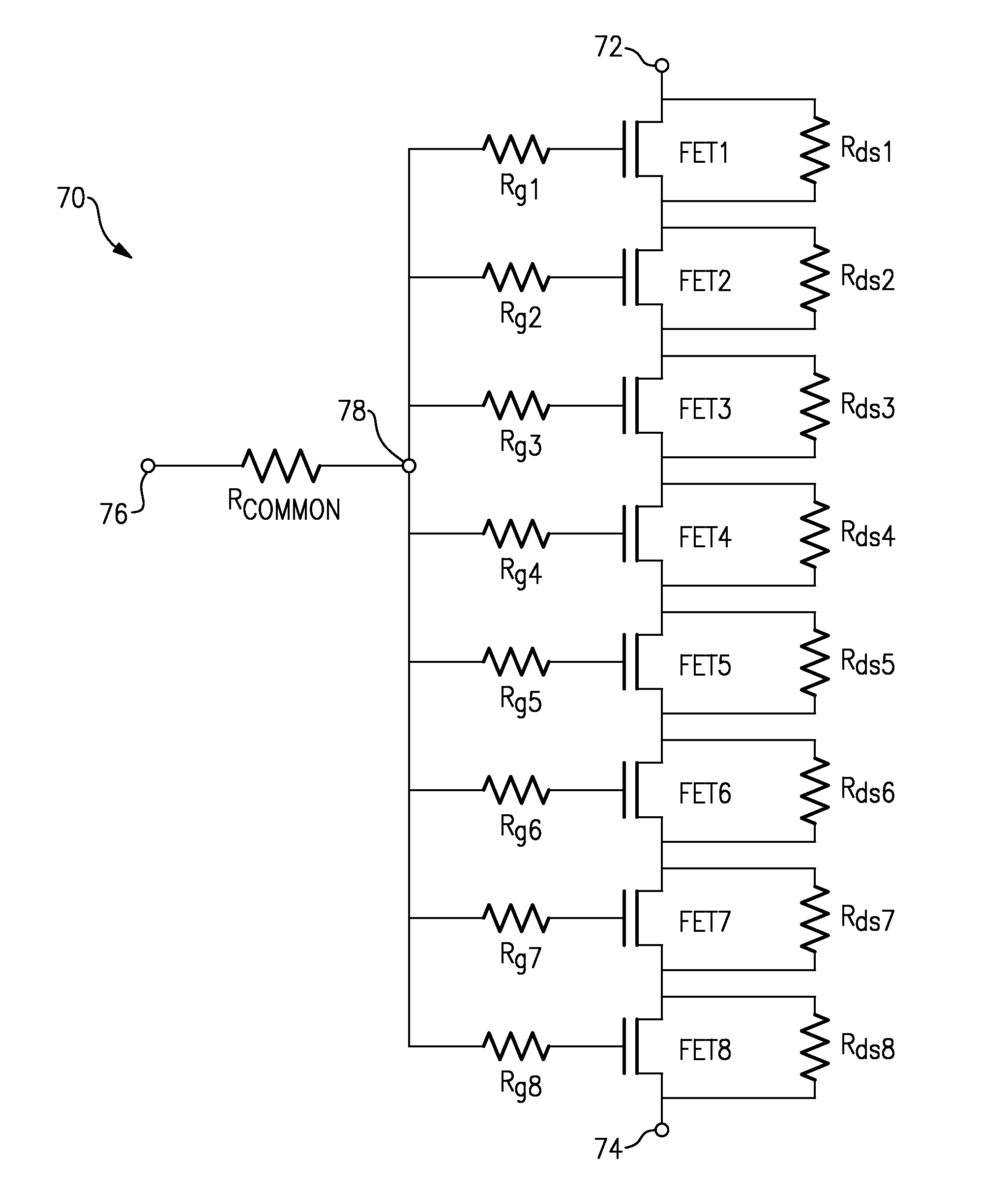
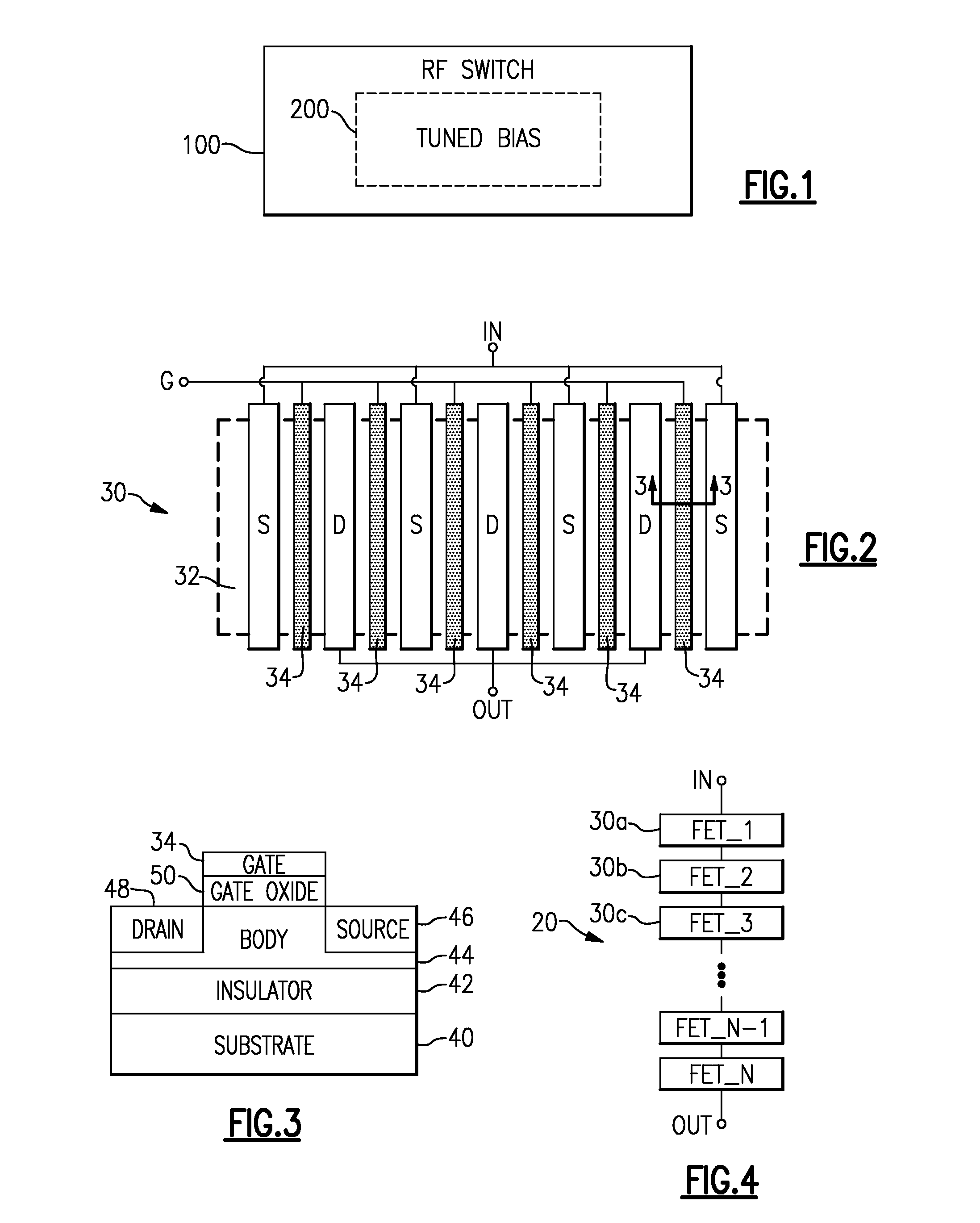
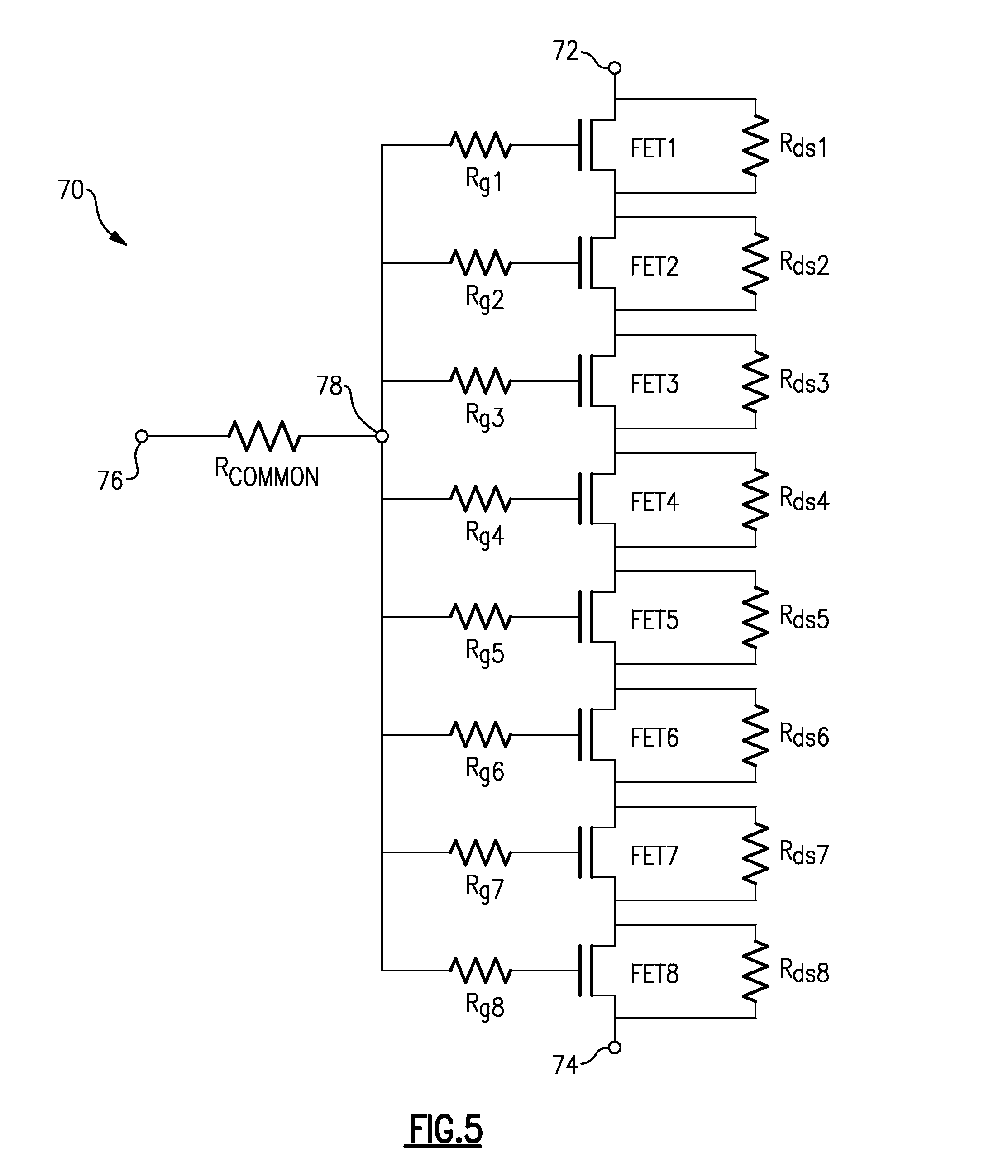
[0048]In some radio-frequency (RF) applications such as antenna tuning or some other switching applications, RF switches and passive components can be utilized. Such RF switches can include a plurality of switching elements (e.g., field-effect transistors (FET)). Such switching elements are commonly arranged in a stack configuration to facilitate appropriate handling of power. For example, a higher FET stack height can be utilized to allow an RF switch to withstand high power under mismatch.

[0049]When such FETs are in an OFF state, they can be thought of as acting as a shunt “high” impedance respect to ground. Such an OFF stack will typically present a capacitance Coff and an impedance Roff that can create mismatch loss (e.g., due to Coff) and / or dissipative loss (e.g., due to Roff). In a situation where a high voltage is applied to the OFF...


PUM


Abstract

Circuits and method for improved quality factor in a stack of transistors. A switching device can include a plurality of field-effect transistors (FETs) implemented in a stack configuration. The switching device can further include a bias circuit having a distribution network that couples a bias input node to the gate of each FET. The distribution network can include a plurality of first nodes, with each first node connected to one or more of the gates through one or more respective resistive paths. The distribution network can further include one or more second nodes, with each second node connected to one or more of the first nodes through one or more respective resistive paths. At least some of the resistive paths can have resistance values selected to reduce loss of a radio-frequency (RF) signal when the FETs are in an OFF state.

Description

CROSS-REFERENCE TO RELATED APPLICATION(S)[0001]This application claims priority to U.S. Provisional Application No. 61 / 903,900 filed Nov. 13, 2013, entitled CIRCUITS AND METHODS FOR IMPROVED QUALITY FACTOR IN A STACK OF TRANSISTORS, the disclosure of which is hereby expressly incorporated by reference herein in its entirety.BACKGROUND[0002]1. Field[0003]The present disclosure generally relates to circuits and methods for improved quality factor in a stack of transistors in radio-frequency (RF) applications.[0004]2. Description of the Related Art[0005]In some radio-frequency (RF) applications, a plurality of switching elements (e.g., field-effect transistors (FETs)) are commonly arranged in a stack configuration to facilitate appropriate handling of power. For example, a higher stack height can be utilized to allow an RF switch to withstand higher power.[0006]When such FETs are in an OFF state, they can be thought of as acting as a shunt “high” impedance respect to ground. Such an OF...

Claims


Application Information

Patent Timeline
Patent Type & Authority Applications(United States)
IPC IPC(8): H03K17/687H01L21/8234
CPCH01L21/8234H03K17/687H04B1/48H03K17/102H03K17/162H01L2224/48091H01L2224/48227H01L2924/15192H01L2924/15313H01L2924/19105H01L2924/13091H01L2924/00
Inventor BLIN, GUILLAUME ALEXANDRE
Owner SKYWORKS SOLUTIONS INC
Why Eureka
Try Eureka