Method for producing strained semi-conductor blocks on the insulating layer of a semi-conductor on insulator substrate

a technology of semi-conductor blocks and insulating layers, which is applied in the direction of semiconductor devices, electrical devices, transistors, etc., can solve the problems of unfavorable p-type transistors, unfavorable p-type transistors, and difficult implementation, and require numerous steps

Active Publication Date: 2015-06-25
COMMISSARIAT A LENERGIE ATOMIQUE ET AUX ENERGIES ALTERNATIVES
View PDF3 Cites 14 Cited by
  • Summary
  • Abstract
  • Description
  • Claims
  • Application Information

AI Technical Summary

Problems solved by technology

Such a strain is however unfavourable to P-type transistors.
Such a method has the drawback of being limited to the tensile straining of Si and to the compressive straining of SiGe, and requiring for this to carry out a growth of SiGe which can prove to be both costly and difficult to implement.
Furthermore, such a method r...

Method used


Image

  • Method for producing strained semi-conductor blocks on the insulating layer of a semi-conductor on insulator substrate
  • Method for producing strained semi-conductor blocks on the insulating layer of a semi-conductor on insulator substrate
  • Method for producing strained semi-conductor blocks on the insulating layer of a semi-conductor on insulator substrate

Examples


Embodiment Construction

[0016]The present invention firstly relates to a method for producing a semi-conductor structure comprising the steps consisting in

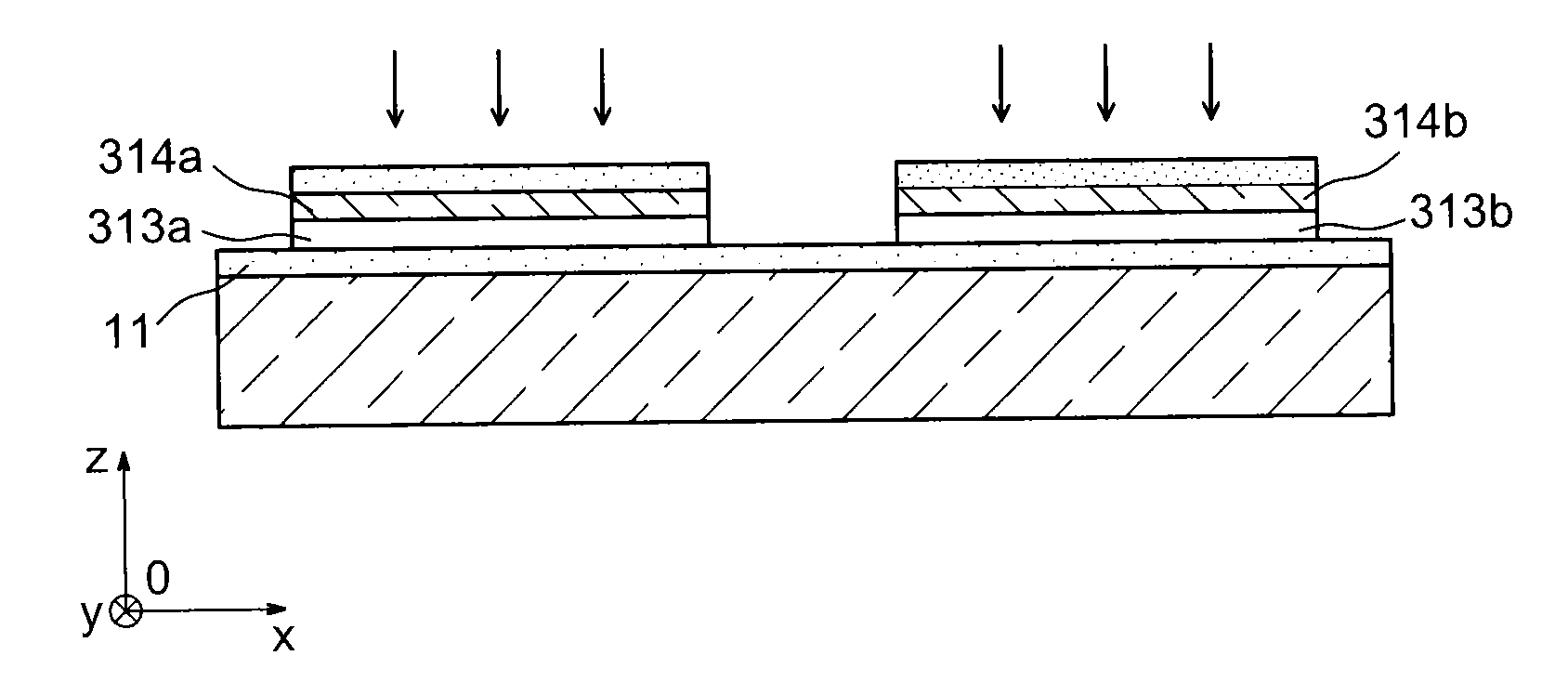
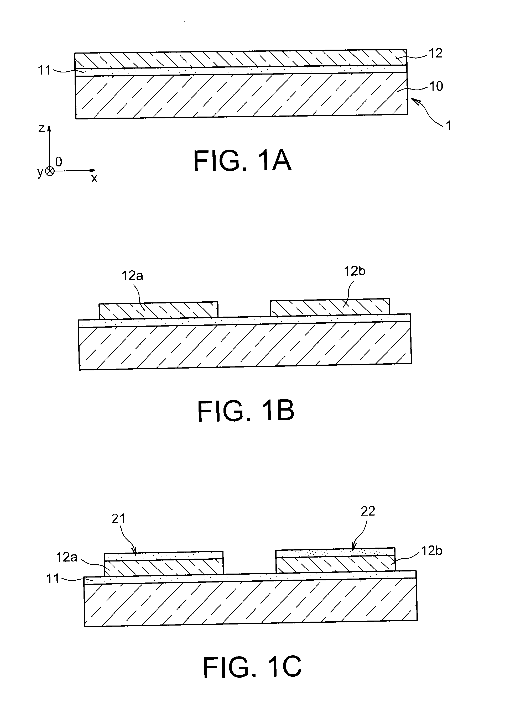
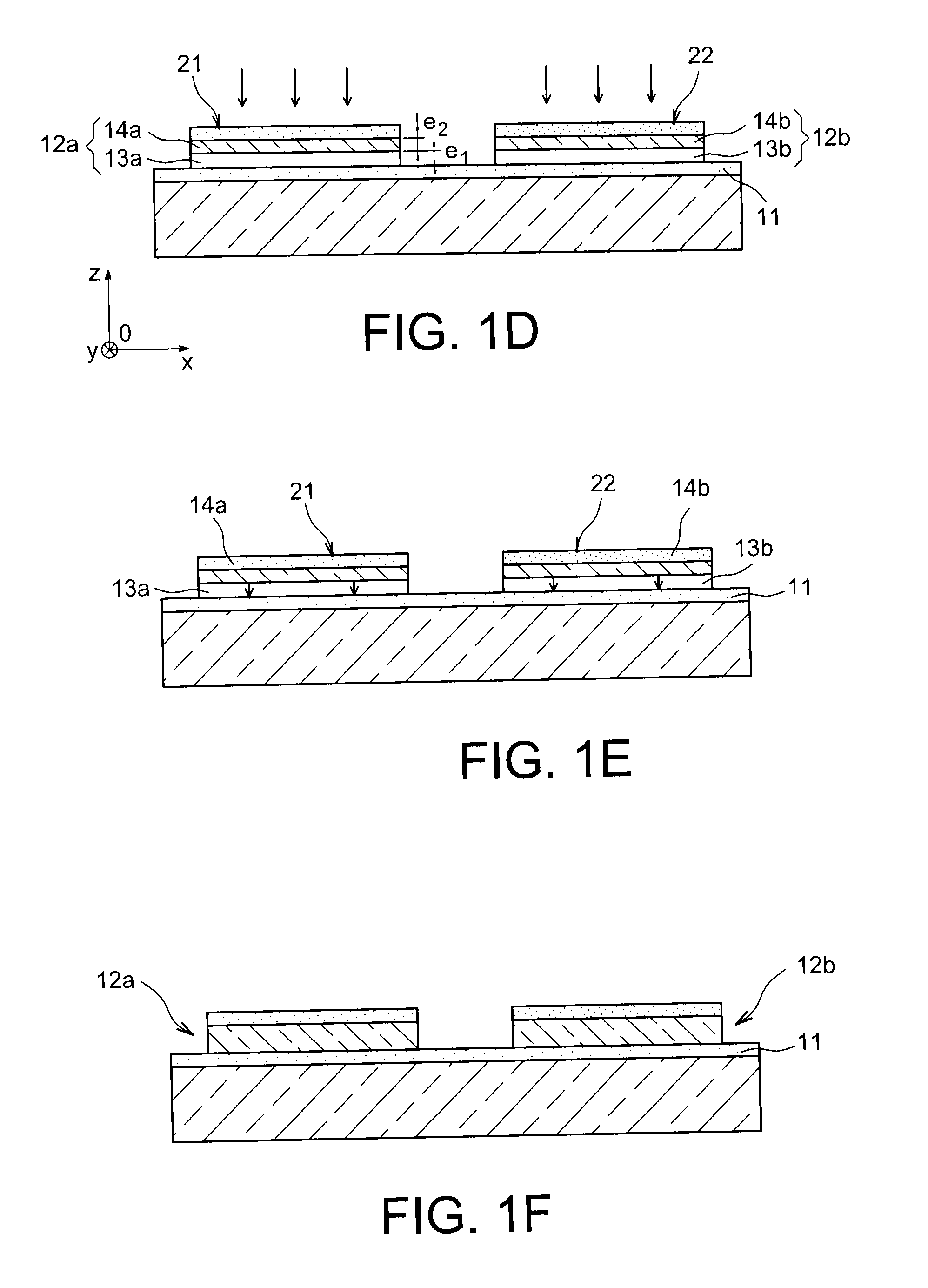
[0017]a) forming on a layer based on amorphous material, a first semi-conductor block covered with a first strain zone based on a tensile strained amorphous material adapted to induce a first strain state in said first block and a second semi-conductor block covered with a second strain zone based on a compressive strained amorphous material adapted to induce a second strain state in said second block, the first block being formed of a lower region based on amorphous semi-conductor material, covered with an upper region of crystalline semi-conductor material in contact with said first strain zone, the second block being formed of a lower region based on amorphous semi-conductor material, the lower region being covered with an upper region of crystalline semi-conductor material in contact with the second strain zone,

[0018]b) recrystallizing the lower regi...


PUM


Abstract

Method for producing a microelectronic device comprising:
a) the formation on an insulating layer of a semi-conductor on insulator type substrate, a first semi-conductor block covered with a first strain zone adapted to induce a compressive strain in said first block and a second semi-conductor block covered with a second strain zone adapted to induce a tensile strain in said second block, the first block and the second block each being formed of a lower region based on amorphous semi-conductor material, covered with an upper region of crystalline semi-conductor material in contact with one of said strain zones,
b) the re-crystallization of said lower region of said first block and of said second block while using said upper region of crystalline material as starting zone for a recrystallization front.

Description

TECHNICAL FIELD AND PRIOR ART[0001]The present description relates to the field of structures formed of a semi-conductor on insulator type substrate, and more particularly that of devices provided with a semi-conductor on insulator type substrate on which several semi-conducting zones having different mechanical strains or undergoing different deformations are formed.[0002]Mechanical deformation is taken to mean a material that has its crystalline lattice parameter(s) lengthened or shortened.[0003]In the case where the deformed lattice parameter is larger than what is termed the “natural” parameter of the crystalline material, this is known as tensile deformation. When the deformed lattice parameter is smaller than the natural lattice parameter, the material is known as compressive deformation.[0004]These mechanical deformation states are associated with mechanical strain states. However, it is also common to refer to these deformation states as mechanical strain states. In the rema...

Claims


Application Information

Patent Timeline
IPC IPC(8): H01L27/12H01L21/306H01L21/762H01L29/78H01L21/84H01L21/02H01L29/04
CPCH01L27/1203H01L21/02422H01L21/30604H01L29/04H01L21/02667H01L21/02609H01L27/092H01L21/02186H01L21/02115H01L29/7843H01L21/84H01L21/76251H01L21/0217H01L21/02532H01L21/26506H01L29/7847H01L21/823807
Inventor REBOH, SHAYBATUDE, PERRINEMAITREJEAN, SYLVAINMAZEN, FREDERIC
Owner COMMISSARIAT A LENERGIE ATOMIQUE ET AUX ENERGIES ALTERNATIVES
Why Eureka
Try Eureka