

Touch panel and method of manufacturing the touch panel
a technology of touch panel and manufacturing method, applied in the field of touch panel, can solve the problems of adverse increase of resistance value of tendency to discontinuity in the routing circuit layer,
- Summary
- Abstract
- Description
- Claims
- Application Information
AI Technical Summary
Benefits of technology
Problems solved by technology
Method used
Image

Examples
first embodiment
(1) First Embodiment
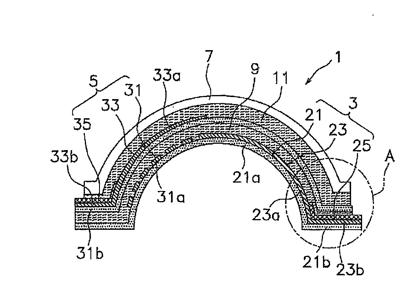
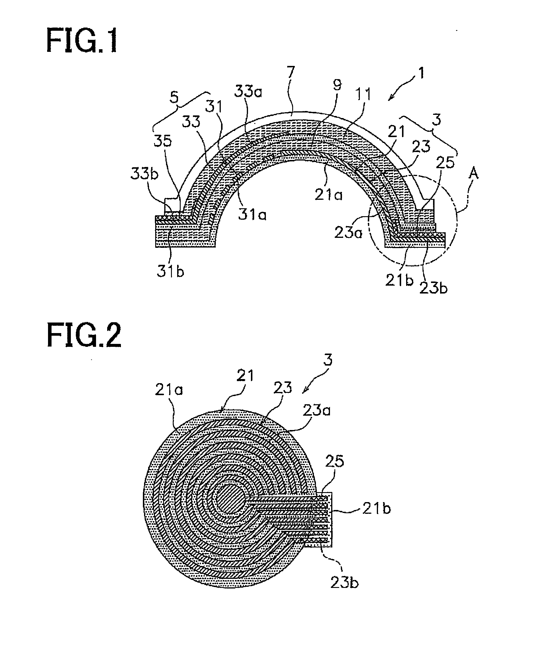
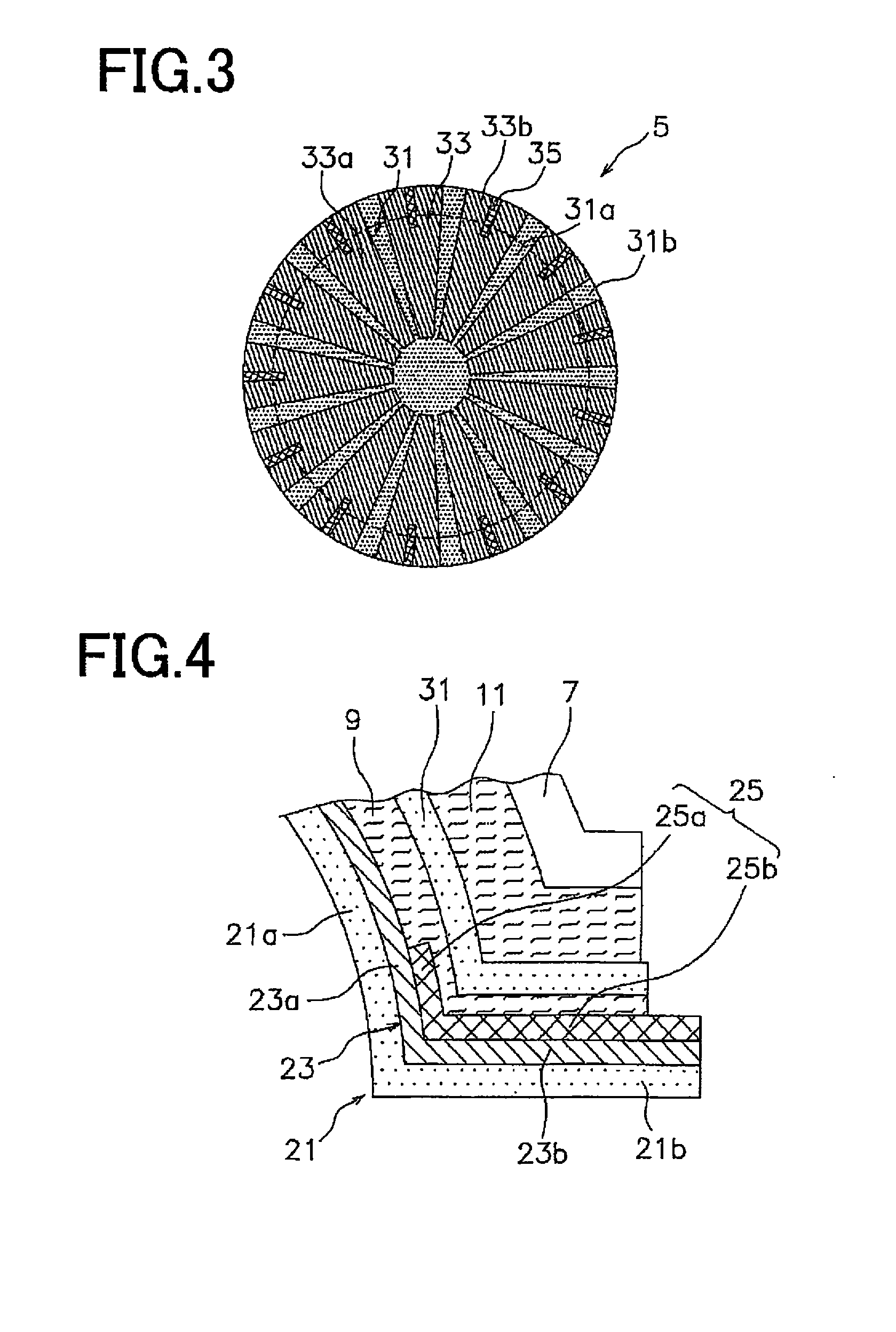
[0070]A touch panel 1 according to one embodiment of the present invention will be explained, referencing FIG. 1 through FIG. 3. FIG. 1 is a cross sectional view of the touch panel. FIG. 2 is a plan view of a first electrode film. FIG. 3 is a plan view of a second electrode film.
[0071]The touch panel 1 is an electrostatic capacitance type touch sensor and has a three dimensional shape, more specifically, a semispherical shape. The touch panel 1 is configured such that XY coordinates are input by an operator touching the touch panel 1 with his or her finger.
[0072]The touch panel 1 principally includes a first electrode film 3, a second electrode film 5, and a protective layer 7. The second electrode film 5 is disposed on the first electrode film 3. The protective layer 7 is disposed on the second electrode film 5. The touch panel 1 further includes a first bonding layer 9 and a second bonding layer 11. The first bonding layer 9 is disposed between the first electr...
second embodiment
(2) Second Embodiment
[0103]An embodiment will be further explained wherein a fluid material is used in the bonding layers and is set after the three dimensional shape has been imparted. In this case, in contrast to the case wherein adhesive sheets are used in the bonding layers, it is assumed that there is a problem in that it is difficult to dispose the bonding layers with even thickness. Accordingly, to solve such a problem, it is conceivable to dispose spacers between the first electrode film and the second electrode film and between the second electrode film and the protective layer, as shown in FIG. 5. In FIG. 5, a plurality of first spacers 41 is formed on the first base material sheet 21, and second spacers 43 are formed on the second base material sheet 31. As a result, the thickness becomes even over the entirety between the first electrode film 3 and the second electrode film 5 and between the second electrode film 5 and the protective layer 7.
third embodiment
(3) Third Embodiment
[0104]Furthermore, in an embodiment wherein a fluid material is used in the bonding layers and the material is set after the three dimensional shape has been imparted, the effect of preventing a discontinuity, even if the routing circuit layers are formed directly on the base material sheets, is achieved, as shown in FIG. 6 through FIG. 8.
[0105]Fourth through eighth embodiments discussed below have in common that, by providing characteristics to the structure of the routing circuit layers, the tensile elongation relative to the tension in the wiring directions is 5% or greater with respect to the locations (hereinbelow, tensile resistant conductive structures) of the routing circuit layers that elongate when the three dimensional shape is imparted to the touch panel. Furthermore, the tensile elongation of the tensile resistant conductive structures relative to tension in the wiring directions is preferably 10% or greater, and is more preferably 15% or greater. Th...
PUM
| Property | Measurement | Unit |
|---|---|---|
| tensile elongation | aaaaa | aaaaa |
| tensile elongation | aaaaa | aaaaa |
| tensile elongation | aaaaa | aaaaa |
Abstract
Description
Claims
Application Information