Thin film transistor substrate and liquid crystal display device using the same

a technology of thin film transistors and liquid crystal display devices, applied in non-linear optics, instruments, optics, etc., can solve the problems of reducing the aperture ratio and the limitation of the application of a recent display device of high resolution, and achieve the effect of improving the aperture ratio and high resolution

Active Publication Date: 2015-07-02
LG DISPLAY CO LTD
View PDF4 Cites 5 Cited by
  • Summary
  • Abstract
  • Description
  • Claims
  • Application Information

AI Technical Summary

Benefits of technology

[0017]An advantage of the present invention is to provide a thin film transistor substrate of which the aperture ratio is improved to be applied to a display device of high resolution, and a liquid crystal display device using the same.
[0018]Additional advantages and features of the invention will be set forth in part in the description which follows and in part will become apparent to those having ordinary skill in the art upon examination of the following. The objectives and other advantages of the various embodiments may be realized and attained by the structure particularly pointed out in the written description and claims hereof as well as the appended drawings.
[0019]To achieve these objects and other advantages, as embodied and broadly described herein, a thin film transistor substrate comprises gate lines arranged on a substrate in a first direction and sub gate lines connected with the gate lines; data lines arranged on the substrate in a second direction to define a pixel including a first pixel and a second pixel, together with the gate lines; a semiconductor layer formed overlapping with each of the gate lines, the sub gate lines and the data lines and connected with the date lines; and a pixel electrode connected with the semiconductor layer.
[0020]In another aspect of the present invention, a liquid crystal display device comprises a thin film transistor substrate; an opposite substrate; and a liquid crystal layer formed between these substrates, wherein the thin film transistor substrate comprises gate lines arranged on a substrate in a first direction and sub gate lines connected with the gate lines; data lines arranged on the substrate in a second direction to define a pixel including a first pixel and a second pixel, together with the gate lines; a semiconductor layer formed overlapping with each of the gate lines, the sub gate lines and the data lines and connected with the date lines; and a pixel electrode connected with the semiconductor layer.

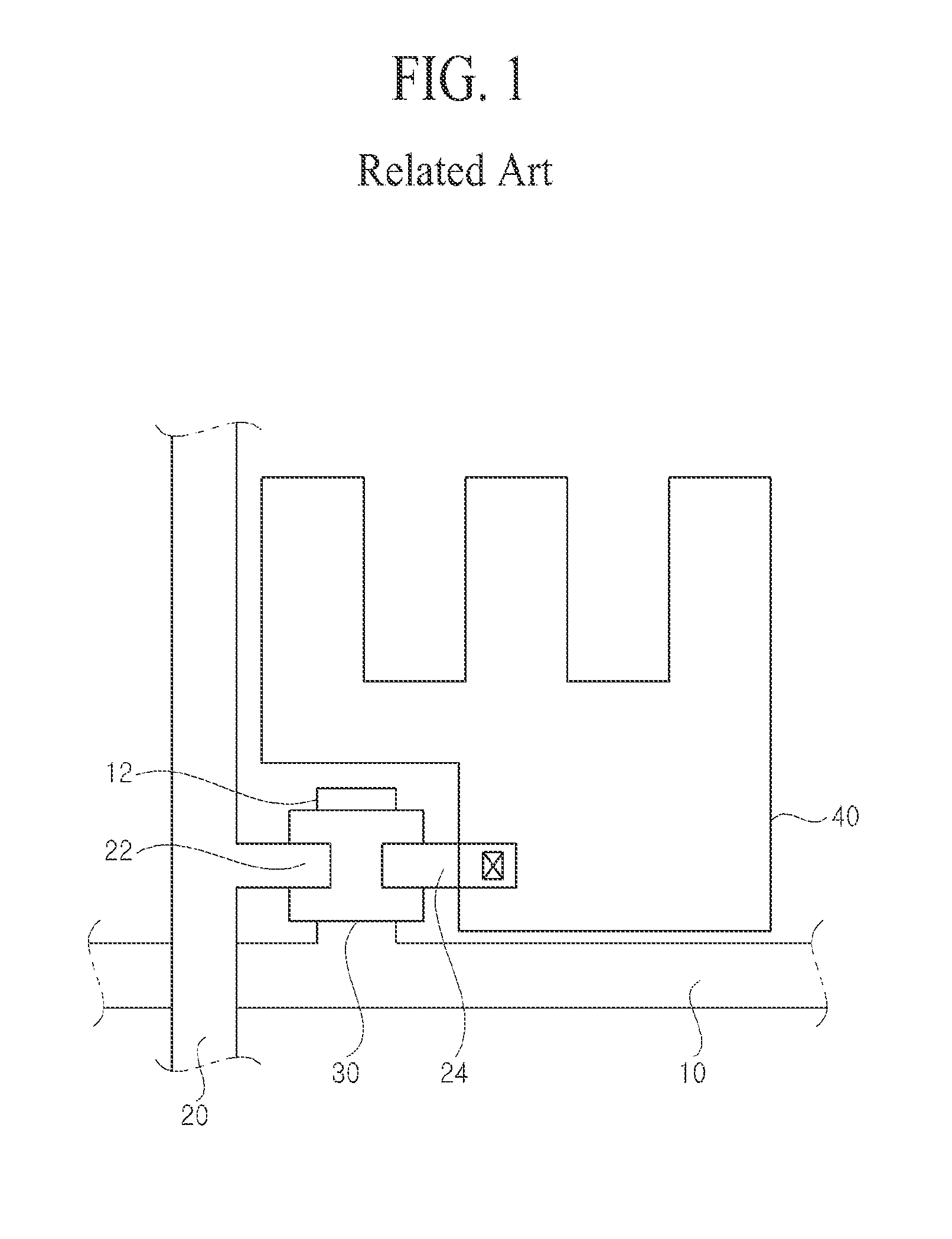
Problems solved by technology

The aforementioned thin film transistor substrate of the related art is used for a display device such as a liquid crystal display device, and has limitation in application for a recent display device of high resolution.
If the structure of the thin film transistor according to the related art is applied to the display device of high resolution, a problem occurs in that an aperture ratio is reduced.

Method used


Image

  • Thin film transistor substrate and liquid crystal display device using the same
  • Thin film transistor substrate and liquid crystal display device using the same
  • Thin film transistor substrate and liquid crystal display device using the same

Examples


Embodiment Construction

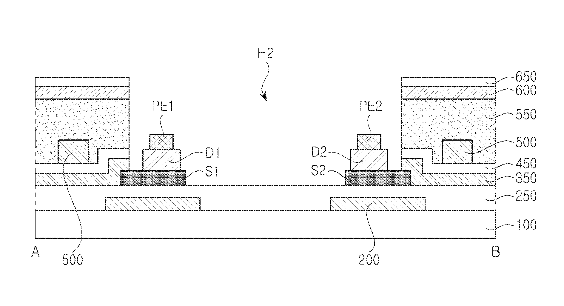
[0029]Reference will now be made in detail to the exemplary embodiments, examples of which are illustrated in the accompanying drawings. Wherever possible, the same reference numbers will be used throughout the drawings to refer to the same or like parts.

[0030]The terminology “on” disclosed in this specification includes the disclosure that an element is formed on a surface of another element and also includes the disclosure that a third element is interposed between the above elements.

[0031]The terminologies such as “first” and “second” disclosed in this specification are not intended to mean the order of corresponding elements but intended to identify one element from another element.

[0032]Hereinafter, various embodiments will be described in detail with reference to the accompanying drawings.

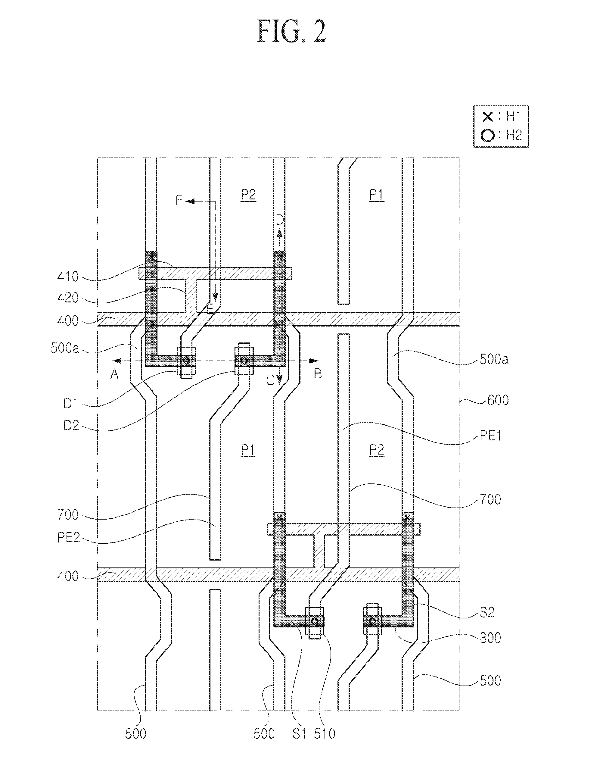
[0033]FIG. 2 is a top view illustrating a thin film transistor substrate according to one embodiment.

[0034]As shown in FIG. 2, the thin film transistor substrate according to one embodiment i...


PUM

PropertyMeasurementUnit
areaaaaaaaaaaa
semiconductoraaaaaaaaaa
gate voltageaaaaaaaaaa

Abstract

A thin film transistor substrate and a liquid crystal display device are disclosed. The thin film transistor substrate comprises gate lines arranged on a substrate in a first direction and sub gate lines connected with the gate lines; data lines arranged on the substrate in a second direction to define a pixel including a first pixel and a second pixel, together with the gate lines; a semiconductor layer formed overlapping with each of the gate lines, the sub gate lines and the data lines and connected with the date lines; and a pixel electrode connected with the semiconductor layer. An aperture ratio may be improved at high resolution.

Description

CROSS REFERENCE TO RELATED APPLICATIONS[0001]This application claims the benefit of the Korean Patent Application No. 10-2013-0166568 filed on Dec. 30, 2013, which is hereby incorporated by reference for all purposes as if fully set forth herein.BACKGROUND OF THE INVENTION[0002]1 . Field of the Invention[0003]The present invention relates to a thin film transistor substrate, and more particularly, to a thin film transistor substrate enabling high resolution of display device.[0004]2. Discussion of the Related Art[0005]A thin film transistor has been widely used as a switching element of a display device such as a liquid crystal display device or an organic light emitting display device.[0006]The thin film transistor includes a gate electrode, a semiconductor layer, a source electrode, and a drain electrode. Hereinafter, a thin film transistor substrate of the related art will be described with reference to the accompanying drawing.[0007]FIG. 1 is a brief plane view illustrating a th...

Claims


Application Information

Patent Timeline
Patent Type & Authority Applications(United States)
IPC IPC(8): H01L27/12G02F1/1362G02F1/1368H01L29/786
CPCH01L27/124G02F1/1368G02F1/136286H01L29/786G02F1/134363H01L29/78645H01L29/78696H01L27/1222G02F1/134372H01L21/18
Inventor JANG, HUNLEE, SUL
Owner LG DISPLAY CO LTD
Why Eureka
Try Eureka