Image sensor

Inactive Publication Date: 2004-08-10
GRAPHIC TECHNO JAPAN
View PDF5 Cites 4 Cited by
  • Summary
  • Abstract
  • Description
  • Claims
  • Application Information

AI Technical Summary

Problems solved by technology

As a result, the CCD image sensor has a problem that the manufacturing process and structure of the CCD image sensor become complicated.
Thus, CMOS image sensor also has a problem that the manufacturing process and structure of the CMOS image sensor be

Method used


Image

  • Image sensor
  • Image sensor
  • Image sensor

Examples


Embodiment Construction

Hereinafter, preferred embodiments of the present invention will be described in detail with reference to the accompanying drawings.

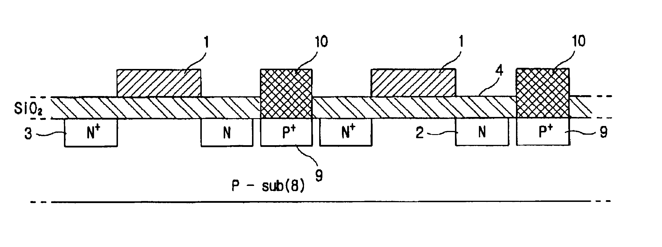
FIG. 3 is a cross-sectional view showing a structure of a unit pixel in an NMOS image sensor in accordance with a preferred embodiment of the present invention.

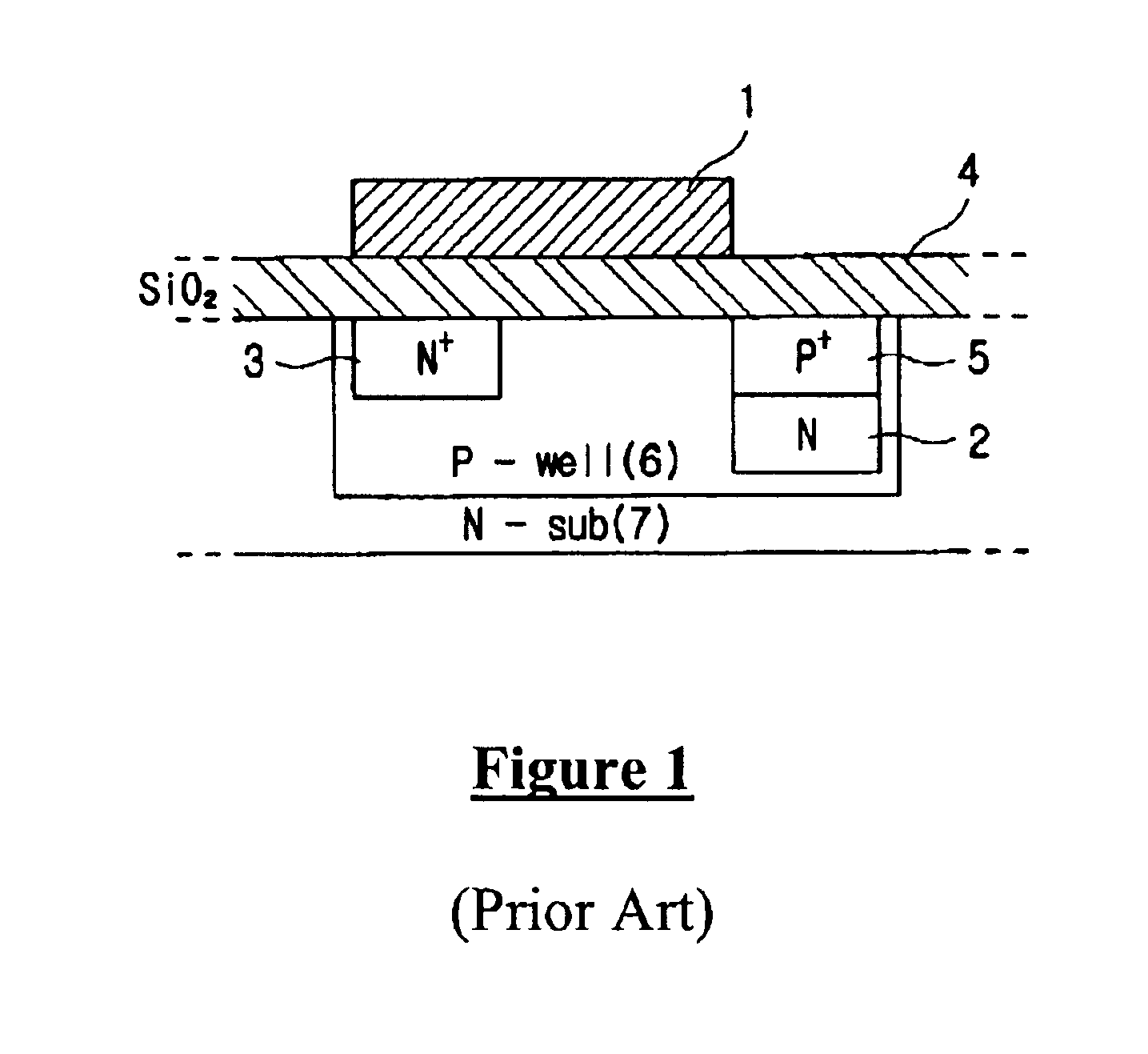
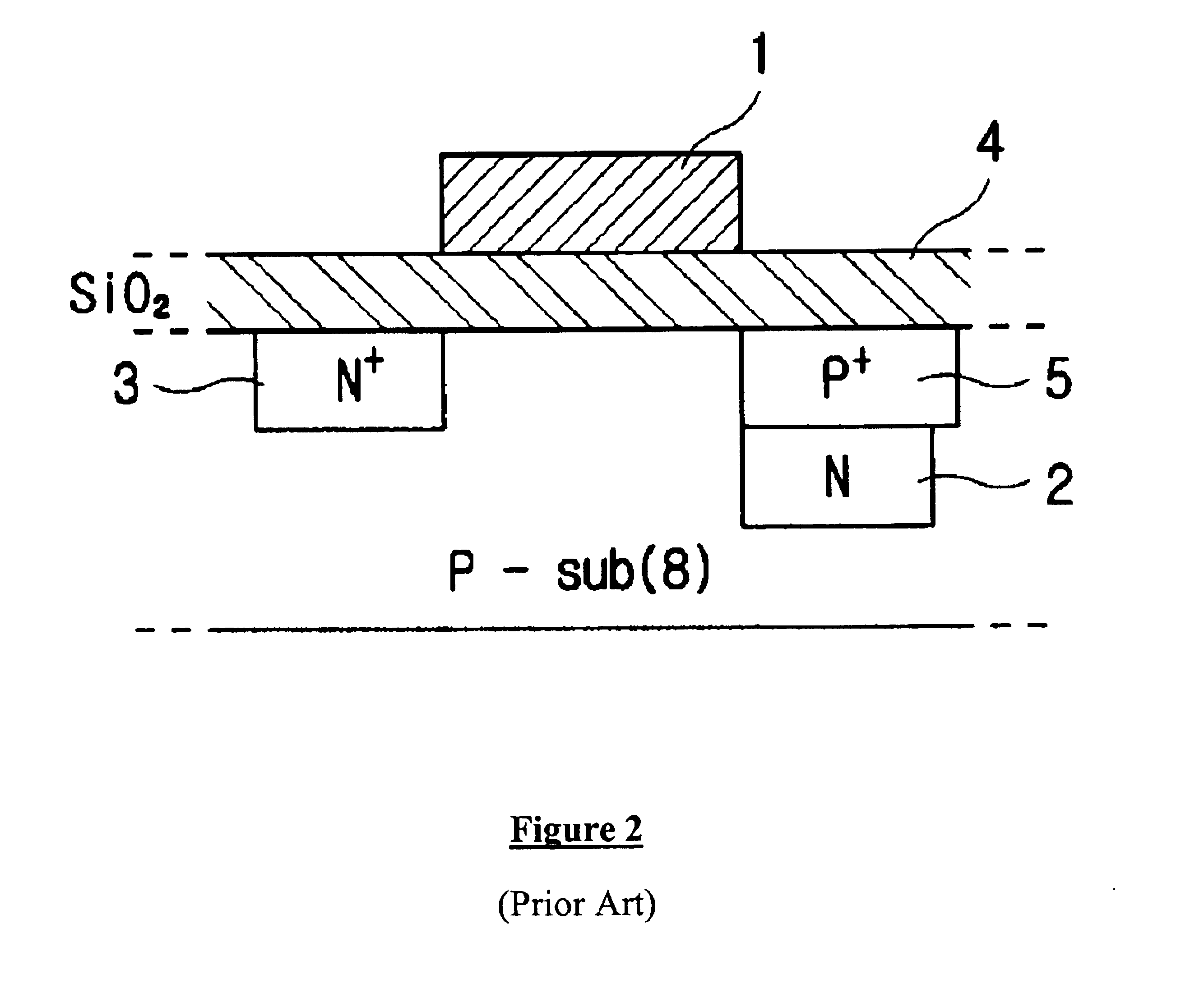
Referring to FIG. 3, the unit pixel of the image sensor in accordance with the present invention includes: an oxide film 4 formed upon a semiconductor substrate 8; a gate electrode 1 formed on the oxide film 4; a photodiode N-type region 2 formed within the semiconductor substrate 8 and having an interface with the oxide film 4, which is spaced apart from the gate electrode 1 by a predetermined distance and disposed on one side of the gate electrode 1; and an N.sup.+ -type region 3 acting as a floating diffusion region, formed within the semiconductor substrate 8 and having an interface with the oxide film 4, which is spaced apart from the gate electrode 1 by a predetermined distance and disposed...


PUM


Abstract

An image sensor with improved productivity and sensitivity is provided. The image sensor includes a plurality of unit pixels, each unit pixel including an oxide film formed upon a semiconductor substrate; a gate electrode formed on the oxide film; a photodiode N-type region formed within the semiconductor substrate and interfacing with the oxide film, which is space apart from the gate electrode by a predetermined distance and disposed on one side of the gate electrode; and a floating diffusion region formed within the semiconductor substrate and interfacing with the oxide film, which is spaced apart from the gate electrode by a predetermined distance and is disposed on the other side of the gate electrode.

Description

1. Field of the InventionThe present invention relates to an image sensor, and more particularly to an image sensor of which productivity and sensitivity are improved.2. Description of the Related ArtConventional image sensors are manufactured in a type of charge coupled device (CCD) or complementary metal-oxide-semiconductor (CMOS) image sensor, which are shown in FIGS. 1 and 2.FIG. 1 is a cross-sectional view showing a structure of a unit pixel in a conventional CCD image sensor.Referring to FIG. 1, the unit pixel of the conventional CCD image sensor includes: an oxide film 4 formed upon a semiconductor substrate 7; a photodiode N-type region 2 formed within the semiconductor substrate 7 at a predetermined depth; a photodiode surface P-type region 5 disposed on the photodiode N-type region 2 and having an interface with the oxide film 4; a floating diffusion region 3 disposed within the semiconductor substrate 7 and having an interface with the oxide film 4, which is spaced apart ...

Claims


Application Information

Patent Timeline
IPC IPC(8): H01L27/146H01L27/148H01L21/00H01L31/0232H01L27/00H01L31/062H01L31/06H01L31/0352
CPCH01L27/14623H01L27/1463H01L27/14643H01L31/0352H01L27/148
Inventor HAYASHIMOTO, YOSHIAKISEO, YOUNG-JOO
Owner GRAPHIC TECHNO JAPAN
Why Eureka
Try Eureka