Thin-film transistor substrate and liquid crystal display

a thin film transistor and substrate technology, applied in the field of thin film transistor substrates and liquid crystal displays, can solve the problems of reducing the aperture ratio, affecting the enhancement of the definition of the display, and affecting the appearance quality of the display, so as to reduce the occurrence of defective displaying and the aperture ratio

Active Publication Date: 2020-05-19
TRIVALE TECH
View PDF37 Cites 5 Cited by
  • Summary
  • Abstract
  • Description
  • Claims
  • Application Information

AI Technical Summary

Benefits of technology

[0009]The present invention has been made to solve the above-described problems, and it is an object of the present invention to provide a thin-film transistor substrate and a liquid crystal display which can suppress occurrence of defective displaying while ensuring an aperture ratio.
[0012]In the thin-film transistor substrate according to one aspect of the present invention, the common electrode need not be placed between the TFT and the pixel electrode formed of a transparent conductive material in a thickness direction. This can allow an electrical path between the TFT and the pixel electrode to be made shorter than that in a case where the common electrode is placed between the TFT and the pixel electrode. This can reduce an area of a contact hole forming the above-stated electrical path, while preventing electrical resistance of the electrical path from excessively increasing. Accordingly, an area of a non-display-pixel area can be reduced. Thus, a high aperture ratio can be easily ensured. Further, firstly, the metal layer including the light-shield part which blocks light travelling toward the channel layer is provided. This suppresses deterioration of the channel layer formed of an oxide semiconductor, which is caused due to light. Thus, defective control of displaying which is caused due to deterioration of the channel layer is suppressed. Secondly, the metal layer, in conjunction with a part of the common electrode, forms a laminated structure. This laminated structure forms an electrical path having low resistance. As a result of this, a potential difference in the common electrode within the TFT substrate is reduced. Thus, unevenness in displaying of a display using the TFT substrate is suppressed. Based on the above-described matters, it is possible to suppress occurrence of defective displaying while ensuring an aperture ratio.
[0013]In the thin-film transistor substrate according to another aspect of the present invention, the common electrode need not be placed between the TFT and the pixel electrode formed of a transparent conductive material in a thickness direction. This can allow an electrical path between the TFT and the pixel electrode to be made shorter than that in a case where the common electrode is placed between the TFT and the pixel electrode. This can reduce an area of a contact hole forming the foregoing electrical path, while preventing electrical resistance of the electrical path from excessively increasing. Accordingly, an area of a non-display-pixel area can be reduced. Thus, a high aperture ratio can be easily ensured. Further, firstly, the metal layer including the light-shield part which blocks light travelling toward the channel layer is provided. This suppresses deterioration of the channel layer formed of an oxide semiconductor, which is caused due to light. Thus, defective control of displaying which is caused due to deterioration of the channel layer is suppressed. Secondly, the metal layer is electrically connected to the gate electrode. This can prevent a high electric field from being generated between the light-shield part included in the metal layer and the gate electrode. Accordingly, the channel layer placed between the light-shield part and the gate electrode can be prevented from being deteriorated due to a high electric field. Thus, defective control of displaying which is caused due to deterioration of the channel layer is further suppressed. Based on the above-described matters, it is possible to suppress occurrence of defective displaying while ensuring a sufficient aperture ratio.

Problems solved by technology

Reduction in aperture ratio hampers enhancement in definition of a display.
Generally, an oxide semiconductor is easily deteriorated due to light such as UV light.
Due to that, defective displaying is likely to occur.
However, to do so results in an increase in an area of a non-display-pixel area.
As described above, in the conventional art, it is difficult to suppress occurrence of defective displaying while ensuring a sufficient aperture ratio.

Method used


Image

  • Thin-film transistor substrate and liquid crystal display
  • Thin-film transistor substrate and liquid crystal display
  • Thin-film transistor substrate and liquid crystal display

Examples


first preferred embodiment

[0027](Configuration of Liquid Crystal Display)

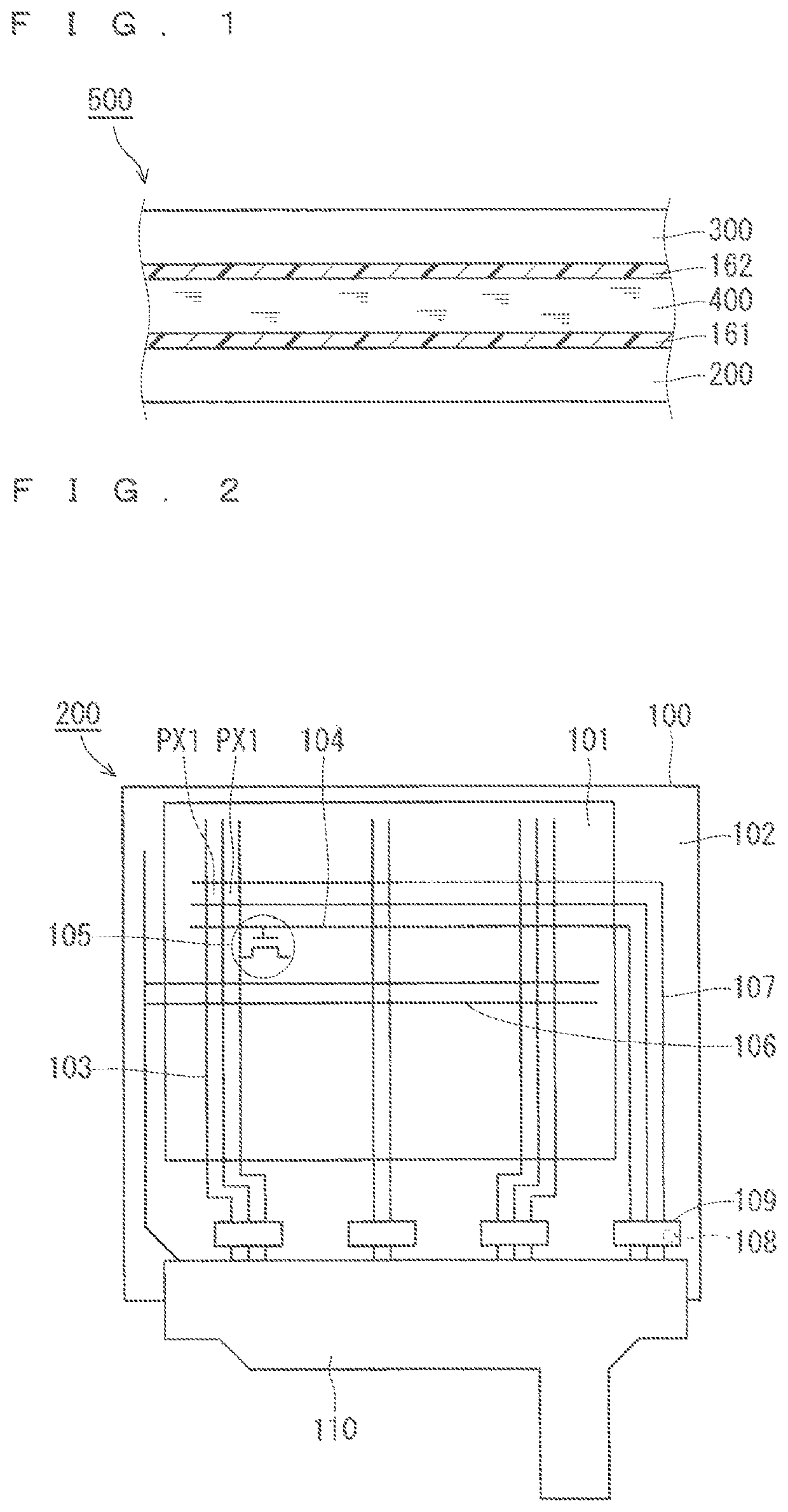
[0028]FIG. 1 is a partial cross-sectional view schematically showing a configuration of a liquid crystal display 500 according to a first preferred embodiment. The liquid crystal display 500 includes a TFT substrate 200 (thin-film transistor substrate), a color filter substrate 300 (counter substrate), a liquid crystal layer 400, an alignment layer 161, and an alignment layer 162. The color filter substrate 300 is placed at a distance from the TFT substrate 200. The liquid crystal layer 400 is held between the TFT substrate 200 and the color filter substrate 300. Each of the alignment layer 161 and the alignment layer 162 serves to cause alignment of the liquid crystal layer 400. The alignment layer 161 and the alignment layer 162 are provided on the TFT substrate 200 and the color filter substrate 300, respectively. In the first preferred embodiment, the liquid crystal display 500 is of a type for an FFS mode.

[0029](Configuration of TF...

second preferred embodiment

[0066]Referring to FIGS. 6 and 7, according to a second preferred embodiment, the TFT substrate 200 (FIGS. 1 and 2) includes a pixel PX2 in place of the pixel PX1 (FIGS. 4 and 5) described in the first preferred embodiment.

[0067]In the pixel PX2, the TFT substrate 200 includes a common transparent conductive layer 106a. The common transparent conductive layer 106a is placed on the insulating film 20. In other words, the common transparent conductive layer 106a is placed in the same layer as the pixel electrode 71. The common transparent conductive layer 106a is provided away from the pixel electrode 71. The common transparent conductive layer 106a is formed of a transparent conductive material. Preferably, the common transparent conductive layer 106a is formed of the same material that forms the pixel electrode 71. In such a case, the common transparent conductive layer 106a and the pixel electrode 71 can be formed simultaneously. This allows the common transparent conductive layer ...

third preferred embodiment

[0072](Configuration)

[0073]Referring to FIGS. 8 and 9, according to a third preferred embodiment, the TFT substrate 200 (FIGS. 1 and 2) includes a pixel PX3, in place of the pixel PX1 (FIGS. 4 and 5) described in the first preferred embodiment.

[0074]In the pixel PX3, a lower gate contact hole 53 (first gate contact hole) which reaches the scanning line 104 is provided in the gate insulating film 2. In the insulating film 20, an upper gate contact hole 122 (second gate contact hole) which is joined to the lower gate contact hole 53 is provided. The upper gate contact hole 122 is formed of the contact hole 52 and the contact hole 62 which are provided in the protective insulating film 5 and the flattening film 6, respectively.

[0075]According to the third preferred embodiment, the metal layer 15 is provided on a part of the flattening film 6 of the insulating film 20, as shown in FIG. 9. In other words, the metal layer 15 is placed in the same layer as the pixel electrode 71. The pixel...


PUM

PropertyMeasurementUnit
relative dielectric constantaaaaaaaaaa
transparentaaaaaaaaaa
thicknessaaaaaaaaaa

Abstract

A channel layer is formed of an oxide semiconductor. A first insulating film is provided on the channel layer, a source line, and a drain electrode, and includes a drain contact hole which reaches the drain electrode. A pixel electrode is provided on the first insulating film, includes a connection conductive layer which is connected to the drain electrode by the drain contact hole, and is formed of a transparent conductive material. The pixel electrode is covered with a second insulating film. A common electrode is provided on the second insulating film, includes an opening which faces the pixel electrode in a thickness direction, and is formed of a transparent conductive material. A metal layer, in conjunction with a part of the common electrode, forms a laminated structure, and includes a light-shield part which overlaps the channel layer at least partially in plan view.

Description

BACKGROUND OF THE INVENTIONField of the Invention[0001]The present invention relates to a thin-film transistor substrate and a liquid crystal display, and particularly to a thin-film transistor substrate and a liquid crystal display which use an oxide semiconductor.Description of the Background Art[0002]A TFT active matrix substrate (or a thin-film transistor substrate, which will hereinafter be referred to as a “TFT substrate”) which uses a plurality of thin-film transistors (TFT) arranged in a matrix, as switching devices, is utilized in an electrooptical apparatus such as a display using liquid crystal (liquid crystal display which will hereinafter be also referred to as an “LCD”), or a display using a light emitting diode (LED) (light-emitting display), for example. As an LCD, a TFT-LCD using a TFT as a switching device and a simple matrix LCD are available, and a TFT-LCD is superior to a simple matrix LCD in display quality. For this reason, a TFT-LCD is widely used in display ...

Claims


Application Information

Patent Timeline
Patent Type & Authority Patents(United States)
IPC IPC(8): G02F1/1362H01L27/12H01L29/786G02F1/136G02F1/1335G02F1/1337G02F1/1343G02F1/1333
CPCG02F1/133512G02F1/136209H01L27/124G02F1/133788H01L27/1225G02F1/136227G02F1/13439G02F1/133345H01L29/78633G02F1/134309G02F1/136286G02F2201/123G02F2001/136218G02F2001/134318G02F2201/121G02F2001/134372G02F2001/13606H01L29/7869G02F1/134318G02F1/13606G02F1/134372G02F1/136218
Inventor KAWABUCHI, SHINJIHOKA, NARUHITOYAMAYOSHI, KAZUSHIHOSONO, AKIHIKOMIYAMOTO, KENICHI
Owner TRIVALE TECH
Why Eureka
Try Eureka