Eureka AIR delivers breakthrough ideas for toughest innovation challenges, trusted by R&D personnel around the world.

Thin film transistor array substrate and method for manufacturing the same

Active Publication Date: 2015-07-02
LG DISPLAY CO LTD
View PDF5 Cites 8 Cited by
  • Summary
  • Abstract
  • Description
  • Claims
  • Application Information

AI Technical Summary

Benefits of technology

The present invention provides a way to make a thin film transistor array substrate that reduces light leakage and compensates for differences in step between display and non-display regions.

Problems solved by technology

When a display device is formed by joining the thin film transistor array substrate to the color filter array substrate, light leakage cannot be completely shielded in a non-display region.
Accordingly, light leakage is generated in adjacent pixel regions and the non-display region, disadvantageously causing deterioration in display quality.

Method used


Image

  • Thin film transistor array substrate and method for manufacturing the same
  • Thin film transistor array substrate and method for manufacturing the same
  • Thin film transistor array substrate and method for manufacturing the same

Examples


Embodiment Construction

[0022]Reference will now be made in detail to the preferred embodiments of the present invention, examples of which are illustrated in the accompanying drawings. Wherever possible, the same reference numbers will be used throughout the drawings to refer to the same or like parts.

[0023]Hereinafter, a thin film transistor array substrate and a method for manufacturing the same according to the present invention will be described in detail with reference to the annexed drawings.

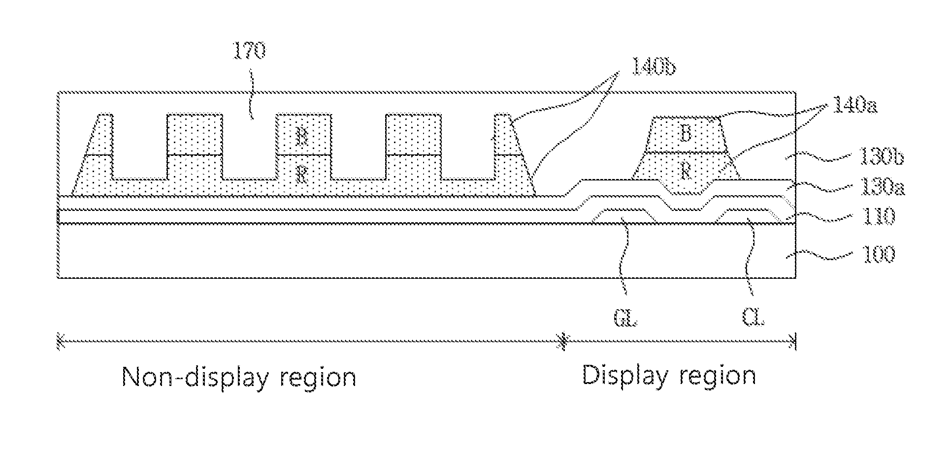
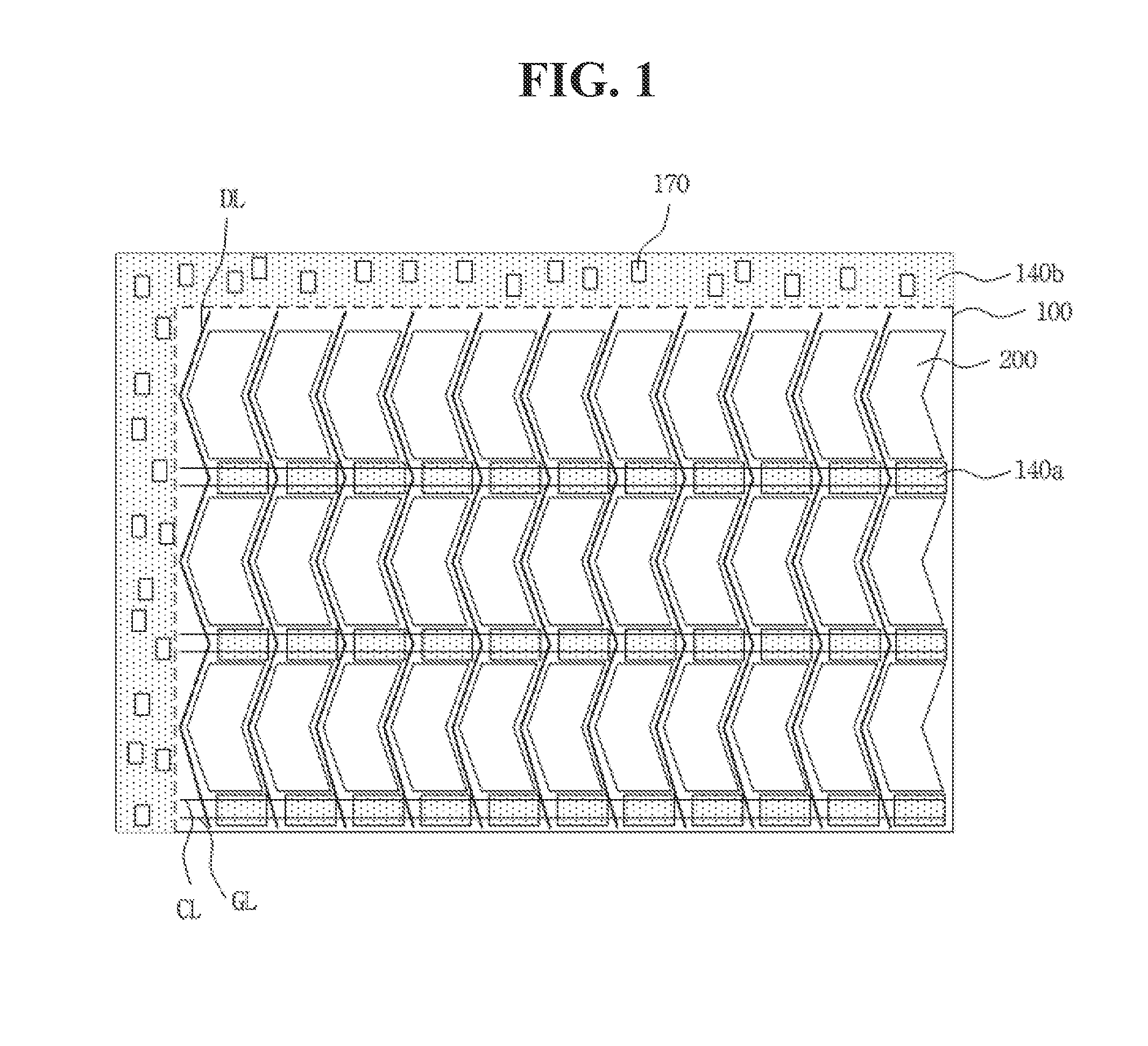
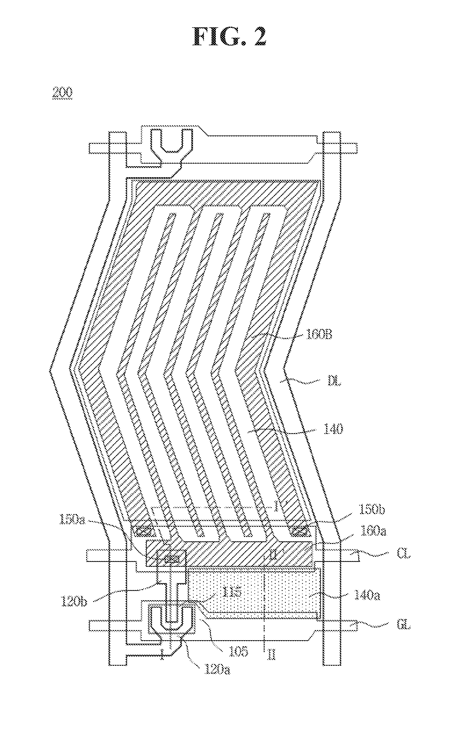
[0024]FIG. 1 is a plan view illustrating a thin film transistor array substrate according to an embodiment of the present invention and FIG. 2 is a plan view illustrating a pixel region of FIG. 1. In addition, FIG. 3A is a cross-sectional view taken along I-I′ of FIG. 2 and FIG. 3B is a cross-sectional view taken along II-II′ of FIG. 2. In addition, FIGS. 4A and 4B are cross-sectional views illustrating a display region and a non-display region according to an embodiment of the present invention.

[0025]As shown i...


PUM


Abstract

To prevent light leakage and compensate for a step between a display region and a non-display region, a thin film transistor array substrate can include a base substrate having a display region and a non-display region, a plurality of pixel regions defined by gate lines and data lines crossing each other in the display region of the base substrate, a common line corresponding to between adjacent pixel regions, a thin film transistor and a color filter in each pixel region, a first dummy color filter between the adjacent pixel regions, a second dummy color filter in the non-display region on the base substrate, the second dummy color filter being provided at an upper surface thereof with at least one recess, and a protective film over the entire surface of the base substrate to cover the first and second dummy color filters and fill the recess.

Description

[0001]This application claims the priority benefit of Korean Patent Application No. 10-2013-0166575, filed on Dec. 30, 2013, which is hereby incorporated by reference as if fully set forth herein.BACKGROUND OF THE INVENTION[0002]1. Field of the Invention[0003]The present invention relates to a thin film transistor array substrate. More specifically, the present invention relates to a thin film transistor array substrate and a method for manufacturing the same to prevent light leakage and to compensate for a step between a display region and a non-display region.[0004]2. Discussion of the Related Art[0005]In accordance with the evolution of information-dependent society, demand for display devices has vastly increased. In response to this demand, in recent years, a variety of display devices such as liquid crystal displays (LCDs), plasma display panels (PDPs), electro-luminescent displays (ELDs) and vacuum fluorescent displays (VFDs) are being researched and some thereof are utilized...

Claims


Application Information

Patent Timeline
IPC IPC(8): H01L27/12
CPCH01L27/1248H01L27/1262H01L27/124G02F1/136286H01L27/1259G02F1/136295G02F1/1362G02F1/133388G02F1/136222H10K59/88H10K59/38G02F1/1335G02F1/136H01L29/786
Inventor KIM, JAE-BUMJUN, WOO-YEALYUN, KYUNG-SUNHAM, YU-JI
Owner LG DISPLAY CO LTD
Why Eureka
Eureka Blog
Learn More