

Use of a (Digital) PUF for Implementing Physical Degradation/Tamper Recognition for a Digital IC
- Summary
- Abstract
- Description
- Claims
- Application Information
AI Technical Summary
Benefits of technology
Problems solved by technology
Method used
Image

Examples
Embodiment Construction
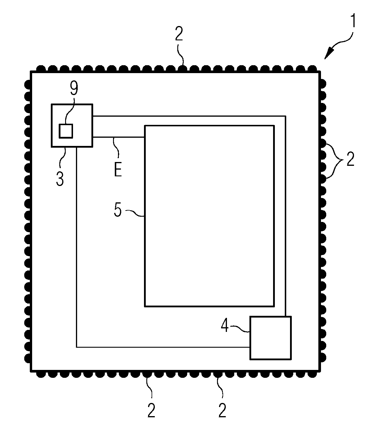
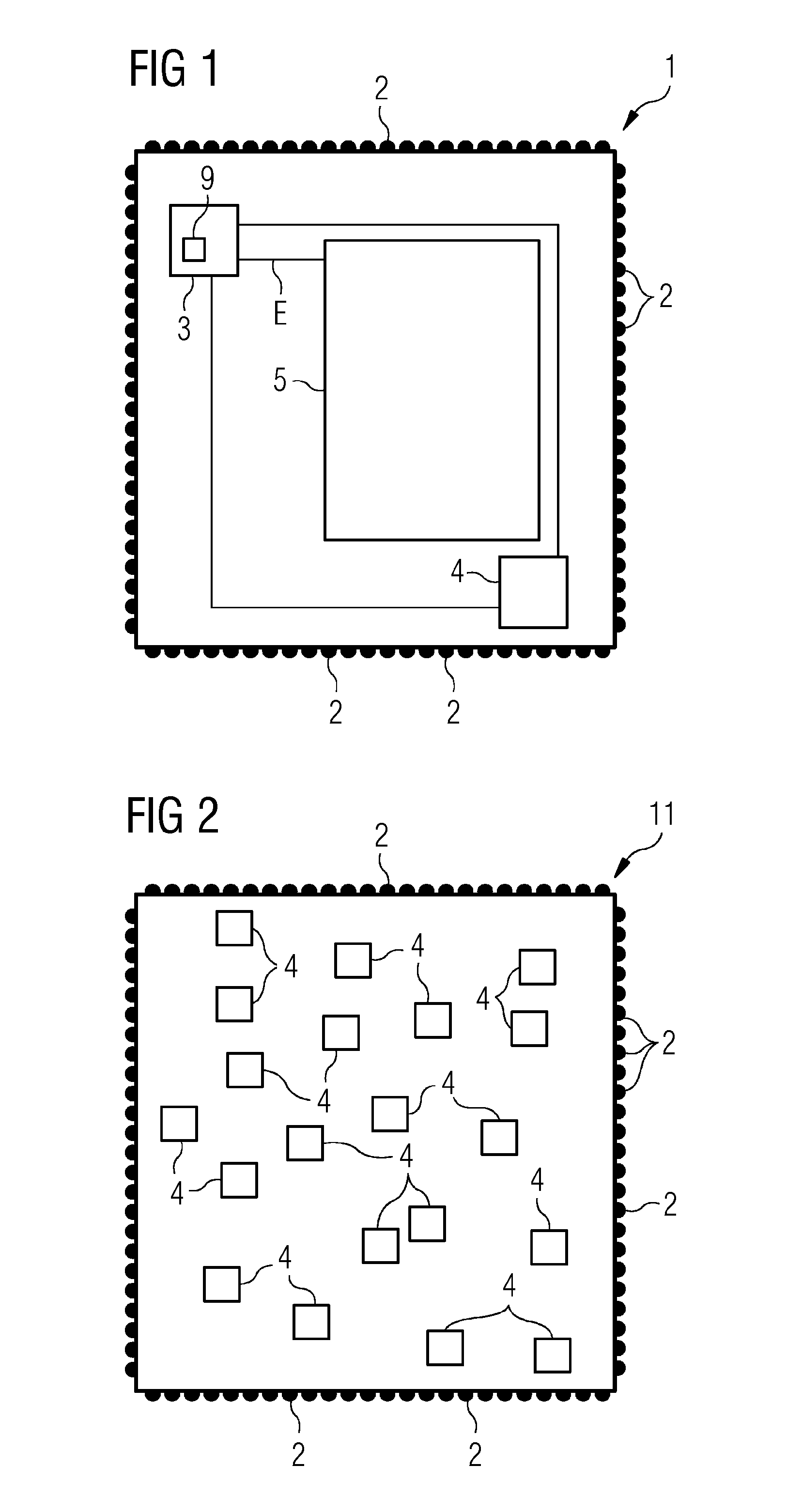
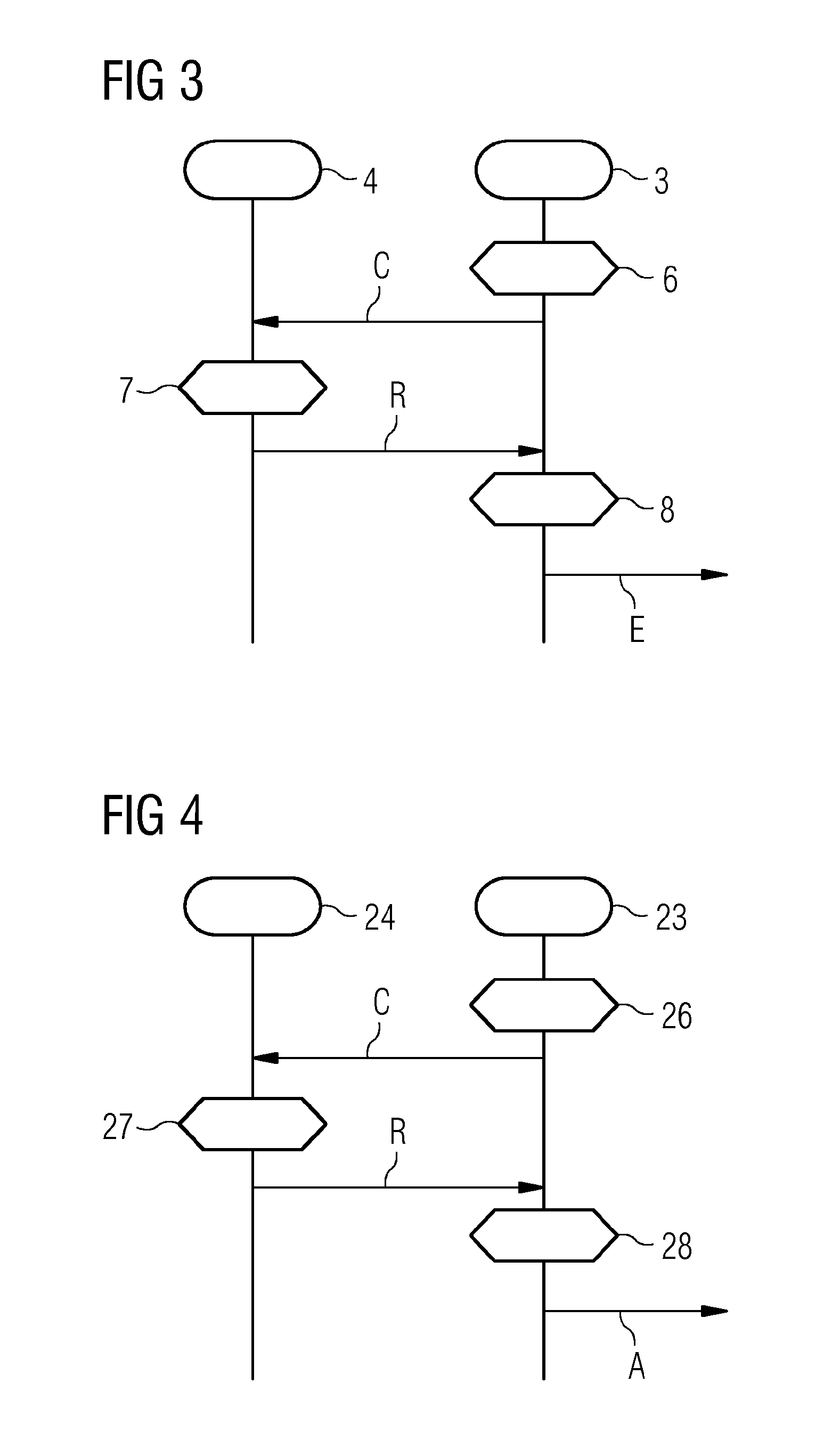
[0053]FIG. 1 shows an example of an integrated circuit 1 (a.k.a. IC, chip, or semiconductor), such as an FPGA or an ASIC, that contains a checking unit 3 (a.k.a. TVU or tamper verification unit). Contacts 2 (a.k.a. pins or interfaces) are shown at the sides of the integrated circuit 1 in FIG. 1. The contacts 2 may be used, for example, to solder the integrated circuit 1 in the form of a chip on a printed circuit board. The TVU 3 detects tampering with the IC 1 by evaluating an integrity sensor 4 (a.k.a. PUF-based tamper sensor, PUF tamper sensor or PTS). Based on a result of the check, an enable signal E is provided. The enable signal is evaluated by a “main function” block 5, for example, to enable or disable a functionality of the IC 1. As a result, a given functionality or the entire IC 1 may be deactivated. In some embodiments, some or all of the external interfaces 2 of the IC 1 may be switched to a “fail safe condition.” In some embodiments, a SafeForUse signal is provided by ...
PUM
 Abstract
Description
Claims
Application Information