Soi finfet with reduced fin width dependence

a technology of finfet and polarizing finfet, which is applied in the field of semiconductor technology, can solve the problems of increasing the difficulty of further reducing, unable to precisely control, and becoming increasingly difficult not only to get a single exact value for the fin width within an entire wafer, or even within a single chip, so as to reduce the off-current spread

Active Publication Date: 2015-07-30
S O I TEC SILICON ON INSULATOR THECHNOLOGIES
View PDF2 Cites 4 Cited by
  • Summary
  • Abstract
  • Description
  • Claims
  • Application Information

AI Technical Summary

Benefits of technology

[0006]This disclosure has been made in view of this problem and it is an object thereof to provide a technology that allows control of the threshold v

Problems solved by technology

However, the minimum dimensions of modern semiconductor technology are such that it is becoming increasingly difficult not only to further reduce them, but also to precisely control them.
In particular, in the field of finfet t

Method used


Image

  • Soi finfet with reduced fin width dependence
  • Soi finfet with reduced fin width dependence
  • Soi finfet with reduced fin width dependence

Examples


Embodiment Construction

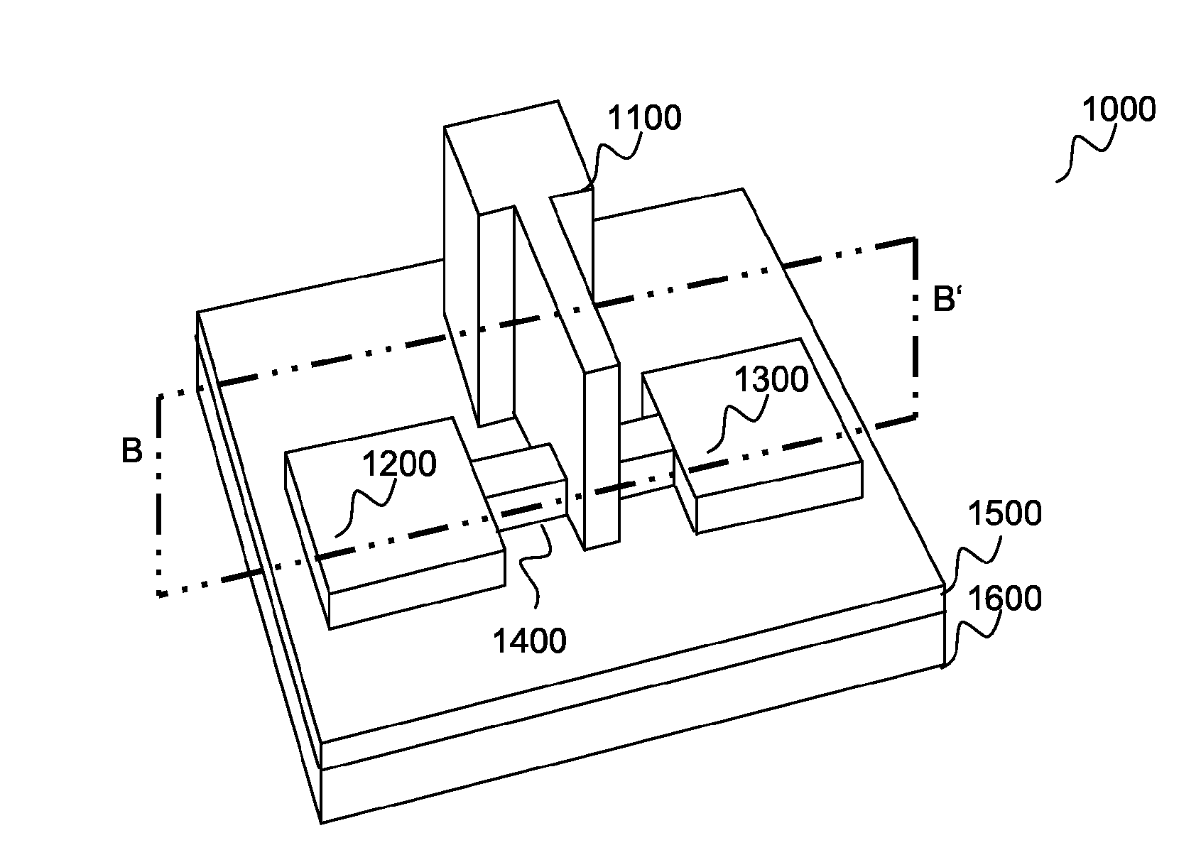
[0019]A finfet 1000 in accordance with an embodiment of the disclosure will now be described with reference to FIG. 1A.

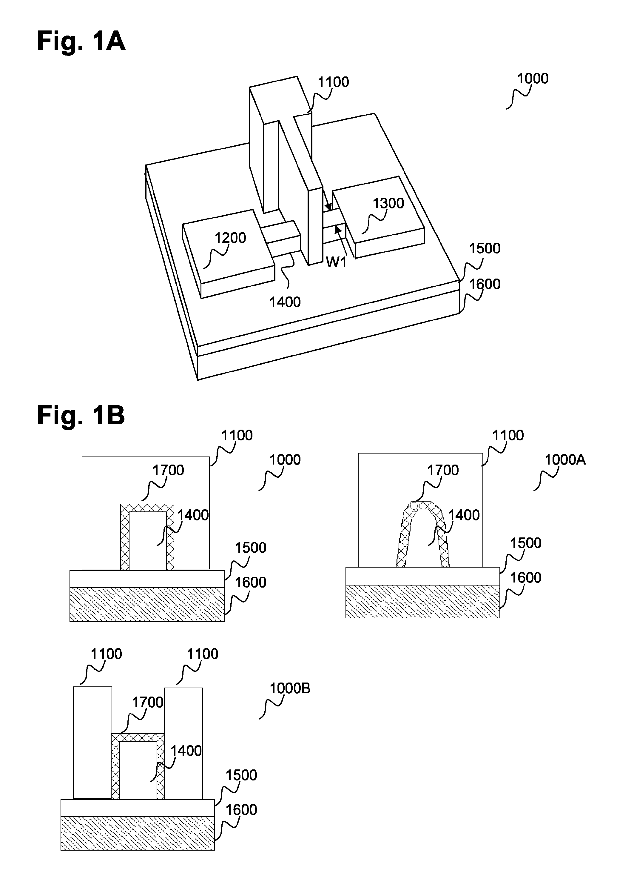
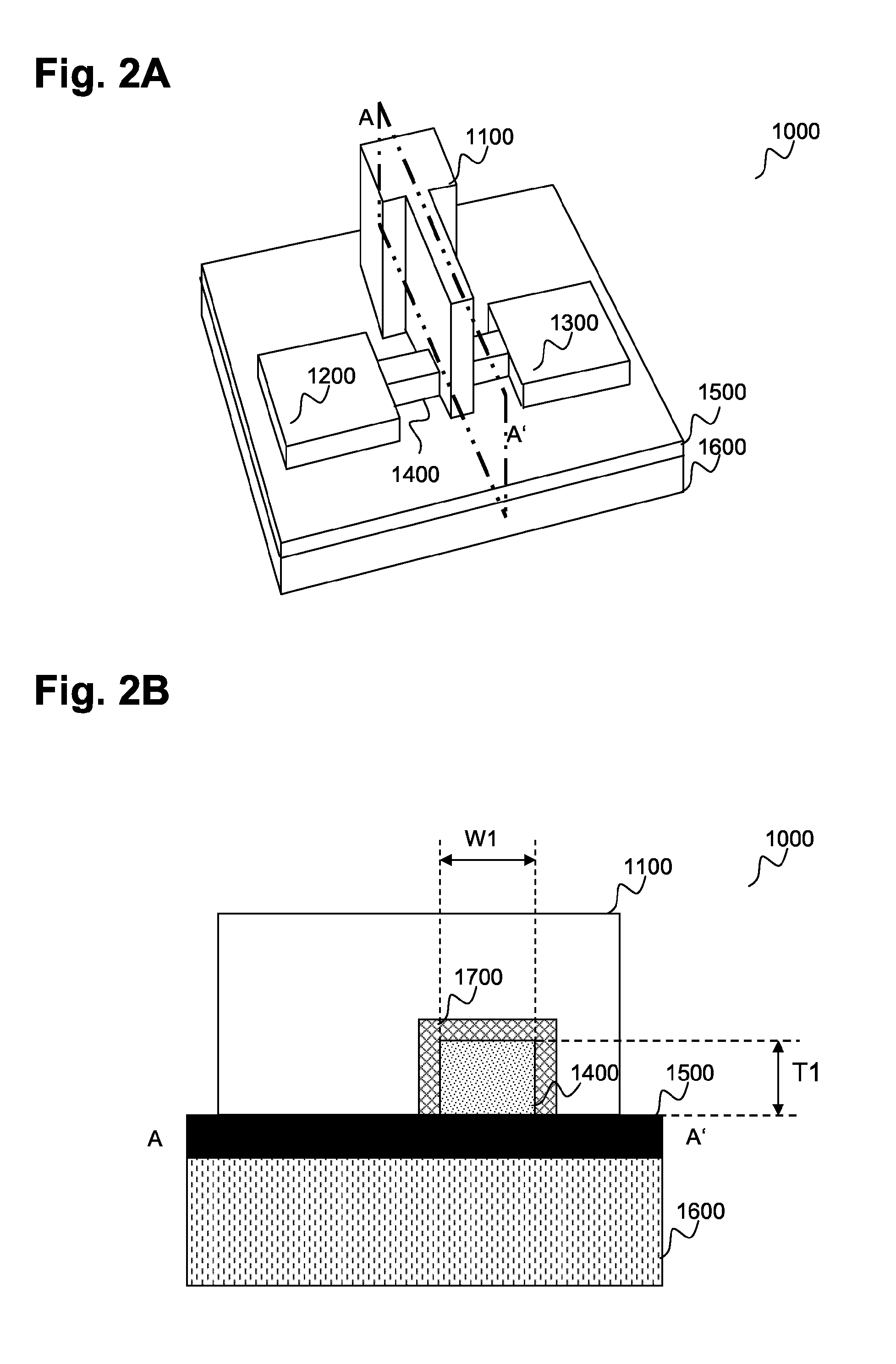
[0020]As can be seen in FIG. 1A, finfet 1000 comprises a gate 1100, a drain 1200, a source 1300 and a silicon and channel region 1400 below the gate. The silicon and channel region 1400 is separated from the gate by insulating layer 1700 (see FIG. 1B). Within the silicon and channel region 1400, a layer close to the insulating layer 1700 acts as channel for conduction of the channel carriers.

[0021]As described above, the width W1 of the silicon and channel region, or fin, can be in the order of 20 nm, or smaller. The finfet 1000 is realized on an insulating layer 1500, separating at least the silicon and channel region 1400 from an underlying semiconductor layer 1600. In particular, the semiconductor layer 1600 can be used as a back gate 1600 for the silicon and channel region 1400, while gate 1100 can be used as a front gate 1100 for silicon and channel region 1400...


PUM


Abstract

The present invention relates to a method for polarizing at least a first finfet transistor and a second finfet transistor, wherein the first finfet transistor has a fin width bigger than the fin width of the second finfet transistor, and both the first finfet transistor and the second finfet transistor have a back gate, and the method comprising applying the same first voltage on the back gate of the first finfet transistor and on the back gate of the second finfet transistor so as to reduce the spread between the off-current value of the first finfet transistor and the off-current value of the second finfet transistor.

Description

CROSS-REFERENCE TO RELATED APPLICATIONS[0001]This application is a national phase entry under 35 U.S.C. §371 of International Patent Application PCT / EP2013 / 068706, filed Sep. 10, 2013, designating the United States of America and published in English as International Patent Publication WO 2014 / 040981 A1 on Mar. 20, 2014, which claims the benefit under Article 8 of the Patent Cooperation Treaty and under 35 U.S.C. §119(e) to French Patent Application Serial No. 1258696, filed Sep. 17, 2012, the disclosure of each of which is hereby incorporated herein in its entirety by this reference.TECHNICAL FIELD[0002]This disclosure relates to the field of semiconductor technology. More specifically, it relates to the field of finfet transistors. Still more specifically, it relates to a method and a corresponding structure for polarizing finfet transistors.BACKGROUND[0003]Semiconductor technology has been following a constant trend of reducing the dimensions of integrated components, such as met...

Claims


Application Information

Patent Timeline
IPC IPC(8): H01L29/78H01L27/12H01L27/02H01L27/088H01L29/66
CPCH01L29/7856H01L27/0886H01L27/1211H01L29/66795H01L27/0214H01L29/7855
Inventor HOFMANN, FRANZ
Owner S O I TEC SILICON ON INSULATOR THECHNOLOGIES
Why Eureka
Try Eureka