
Anti-slip end-effector for transporting workpiece

Active Publication Date: 2015-08-06
ASM IP HLDG BV
View PDF20 Cites 333 Cited by
  • Summary
  • Abstract
  • Description
  • Claims
  • Application Information

AI Technical Summary

Problems solved by technology

When the transferring speed is increased, since the wafer stays on the end effector by friction, the wafer sometimes move

Method used


Image

  • Anti-slip end-effector for transporting workpiece
  • Anti-slip end-effector for transporting workpiece
  • Anti-slip end-effector for transporting workpiece

Examples


example 1

[0052]The following pins having a cross section illustrated in FIG. 4 (except that the surface roughness varied and the thickness of the head part was 1.5 mm) were prepared:

[0053](1) Pins made of Al2O3 having a top face with a surface roughness (Ra) of 0.4 μm and a spherical radium (SR) of 10 mm.

[0054](2) Pins made of polybenzimidazole (PBI) having a top face with an Ra of 0.05 μm and a SR of 10 mm.

[0055](3) Pins made of PBI having a top face with an Ra of 0.4 μm and a SR of 10 mm.

[0056](4) Pins made of PBI (with shot blasting treatment) having a top face with an Ra of 1.2 μm and a SR of 10 mm.

[0057]Four pins of each type were installed on a wafer stage of a static friction coefficient measuring device illustrated in FIG. 8. A 300-mm Si wafer was placed on the wafer stage with the pins, and by lifting the wafer stage, a sliding angle θ at which the wafer started sliding was measured as illustrated in FIG. 9. The static friction coefficient was calculated as tan θ. The above static f...

example 2

[0060]The following pins having a cross section illustrated in FIG. 4 (except that the spherical radius varied and the thickness of the head part was 1.5 mm) were prepared:

[0061](5) Pins made of PBI having a top face with an Ra of 0.05 μm and a spherical radius (SR) of 2.5 mm.

[0062](6) Pins made of PBI having a top face with an Ra of 0.05 μm and a SR of 20 mm.

[0063]Four pins of each type were installed on the wafer stage of the static friction coefficient measuring device illustrated in FIG. 8. A 300-mm Si wafer was placed on the wafer stage with the pins, and by lifting the wafer stage, a sliding angle θ at which the wafer started sliding was measured as illustrated in FIG. 9. The static friction coefficient was calculated as tan θ. The above static friction coefficient measuring steps were continuously repeated. FIG. 6 is a graph showing changes of static friction coefficient of pins (5) (SR 2.5), pins (6) (SR 20), and pins (2) (SR 10) (which were used in Example 1) in relation to...

example 3

[0066]The following pins having a cross section illustrated in FIG. 4 (except that the spherical radius was 10 mm, the thickness of the head part was 1.5 mm, and a surface roughness was 0.4 μm) were prepared:

[0067](7) Pins made of Al2O3

[0068](8) Pins made of PBI (CELAZOLE®).

[0069](9) Pins made of quartz.

[0070]Four pins of each type were installed on the wafer stage of the static friction coefficient measuring device illustrated in FIG. 8. A 300-mm Si wafer was placed on the wafer stage with the pins, and by lifting the wafer stage, a sliding angle θ at which the wafer started sliding was measured as illustrated in FIG. 9. The static friction coefficient was calculated as tan θ. The above static friction coefficient measuring steps were continuously repeated 60 times. The same steps were conducted using a 300-mm Si wafer having a different film formed thereon. FIG. 7 is a graph showing changes of static friction coefficient of pins (7) (Al2O3), pins (8) (CELAZOLE), and pins (9) (qua...


PUM

PropertyMeasurementUnit
Lengthaaaaaaaaaa
Radiusaaaaaaaaaa
Surface roughnessaaaaaaaaaa

Abstract

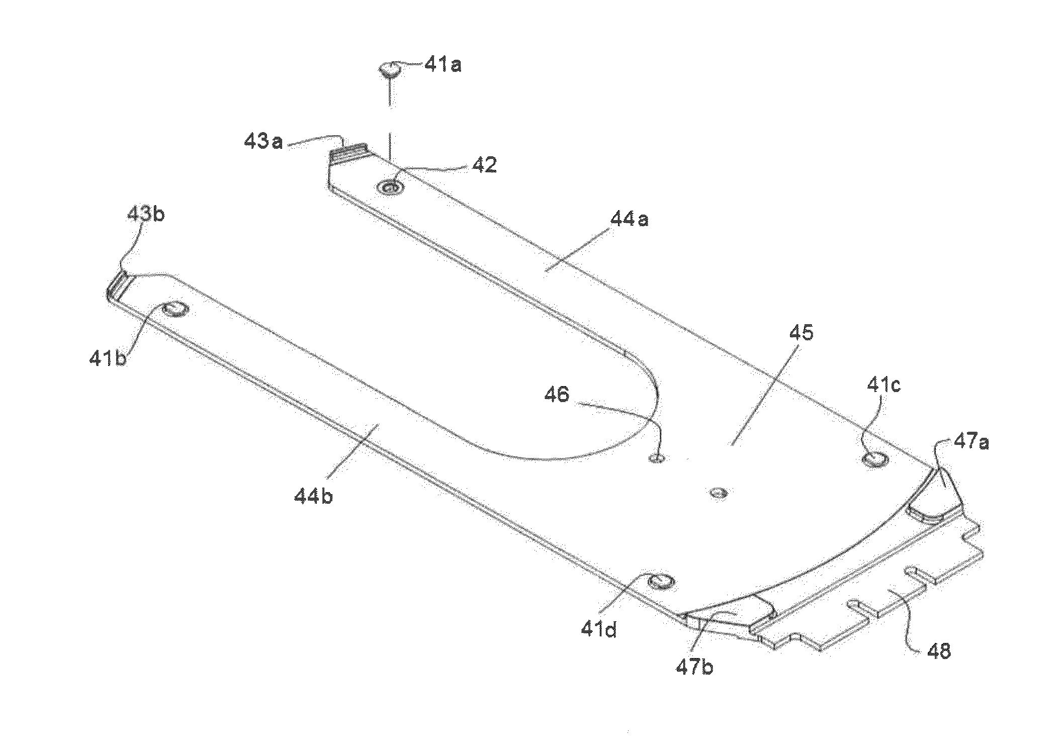
An anti-slip end-effector for transporting a workpiece, which is configured to be attached to a robotic arm, includes: a workpiece-supporting area for placing a workpiece thereon for transportation; at least one front protrusion disposed at a distal end of the workpiece-supporting area for engaging an edge of the workpiece to restrict movement of the workpiece placed on the workpiece-supporting area beyond the front protrusion; and at least one anti-slip protrusion disposed in the workpiece-supporting area for contacting and supporting the backside of the workpiece, said anti-slip protrusion having a top face having a static friction coefficient of 1.0 or more as measured against the backside of the workpiece, and having a surface roughness of less than 0.4 μm.

Description

BACKGROUND OF THE INVENTION[0001]1. Field of the Invention[0002]The present invention generally relates to an end effector for transporting a workpiece such a semiconductor wafer between a transferring chamber and a processing chamber for processing a workpiece, for example.[0003]2. Description of the Related Art[0004]A process of semiconductor manufacturing includes a step of transporting a semiconductor wafer from a wafer-storing cassette to a processing chamber via a transferring chamber using a robotic arm or a step of transporting a semiconductor wafer from a processing chamber to another processing chamber using a robotic arm. The robotic arm is provided with an end effector for loading a wafer thereon and carrying the wafer from one chamber to another. Typically, the end effector does not have a mechanical clamping mechanism for clamping a wafer, and by a wafer positioning or alignment mechanism (e.g., those disclosed in U.S. Patent Application Publication No. 2012 / 0325148, U...

Claims


Application Information

Patent Timeline
IPC IPC(8): B25J15/00H01L21/677B25J11/00
CPCB25J15/0014H01L21/677B25J15/0085B25J11/0095H01L21/67742H01L21/68707Y10T29/49998
Inventor TSUJI, NAOTOYAMAGISHI, TAKAYUKI
Owner ASM IP HLDG BV
Learn More