Solid-state imaging device and camera module

Inactive Publication Date: 2015-08-06
SOVEREIGN PEAK VENTURES LLC
View PDF4 Cites 55 Cited by
  • Summary
  • Abstract
  • Description
  • Claims
  • Application Information

AI Technical Summary

Benefits of technology

[0025]According to the present invention, an infrared cut filter and an infrared transmission filter according to sensitivity of the human eye are formed inside a solid-state imaging device. Thus, the solid-state imaging device can simultaneously image visible light and near-infrar

Problems solved by technology

Accordingly, without an infrared cut filter, near-infrared signals are mixed into red, green, and blue signals due to the influence of infrared light, resulting in a picture having an unnat

Method used


Image

  • Solid-state imaging device and camera module
  • Solid-state imaging device and camera module
  • Solid-state imaging device and camera module

Examples


first embodiment

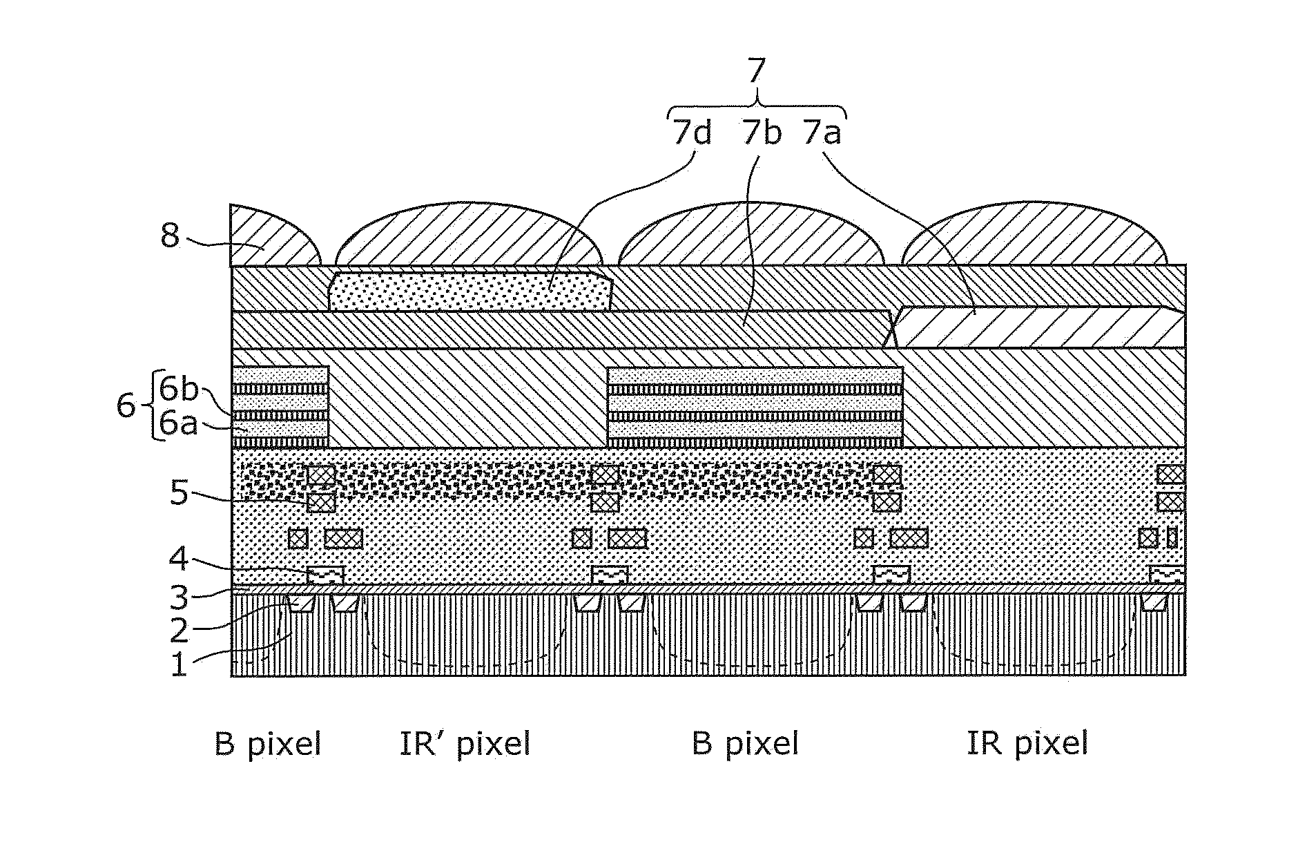
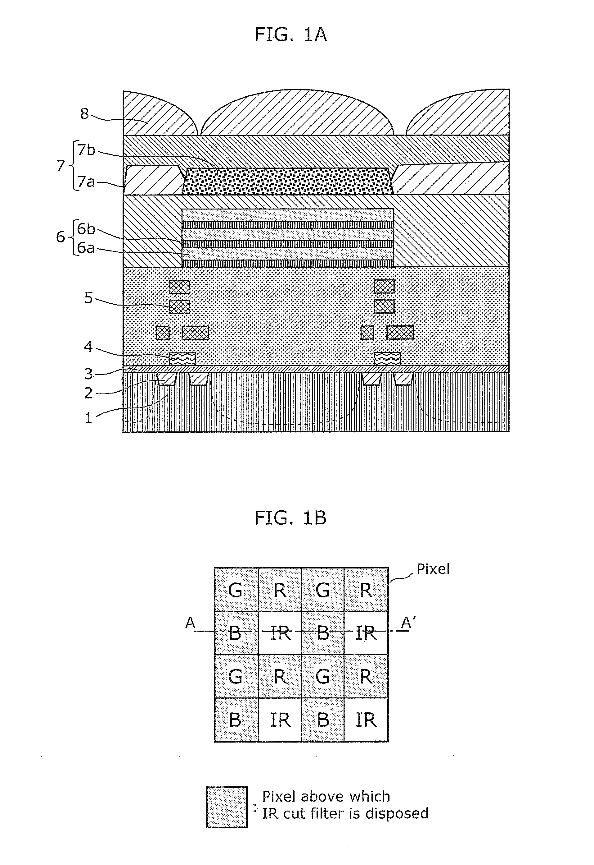
[0059]FIG. 1A is a cross-sectional view illustrating a schematic structure of a solid-state imaging device according to a first embodiment, and FIG. 1B is a plan view illustrating the layout of pixels (arrangement of color filters) of the solid-state imaging device according to the first embodiment. It should be noted that FIG. 1A illustrates a cross-sectional view taken along a portion of the dashed dotted line (line A-A′) of FIG. 1B. In addition, the rectangles illustrated in FIG. 1B represent regions corresponding to pixels. The symbols “R”, “G”, and “B” indicate pixels which detect red, green, and blue light, respectively, and the symbol “IR” indicates a pixel which detects infrared rays (in particular, near-infrared rays). In the following, in order to simplify the description, pixels which detect red, green, and blue light are referred to as a red pixel, a green pixel, and a blue pixel, respectively, and a pixel which detects infrared rays is referred to as an infrared pixel.

[...

second embodiment

[0113]FIG. 9A is a cross-sectional view illustrating a schematic structure of a solid-state imaging device according to a second embodiment, and FIG. 9B is a plan view illustrating the layout of pixels of the solid-state imaging device according to the second embodiment. It should be noted that FIG. 9A illustrates a cross-sectional view taken along a portion of the dashed dotted line (line A-A′) of FIG. 9B. In addition, the rectangles illustrated in FIG. 9B represent regions corresponding to pixels. In addition, in FIG. 9B, the symbols “R”, “G”, and “B” indicate a red pixel, a green pixel, and a blue pixel, respectively, and the symbols “IR” and “IR” indicate a first infrared pixel and a second infrared pixel having different spectral characteristics. A basic structure of the solid-state imaging device according to the present embodiment is similar to that according to the first embodiment, and thus the following gives a description focusing on the differences between the first and ...

third embodiment

[0126]FIG. 11A is a cross-sectional view illustrating a schematic structure of a solid-state imaging device according to a third embodiment, and FIG. 11B is a plan view illustrating the layout of pixels of the solid-state imaging device according to the third embodiment. It should be noted that FIG. 11A illustrates a cross-sectional view taken along a portion of the dashed dotted line (line A-A′) in FIG. 11B. In addition, the rectangles illustrated in FIG. 11B indicate regions corresponding to the pixels. In FIG. 11B, the symbols “R”, “G”, and “B” indicate a red pixel, a green pixel, and a blue pixel, respectively, and the symbol “W” indicates a white pixel which detects infrared rays and visible light. In addition, the basic structure of the solid-state imaging device according to the present embodiment is similar to those according to the first and second embodiments, and thus the following briefly describes the differences from the first and second embodiments.

[0127]The solid-sta...


PUM


Abstract

A solid-state imaging device includes: a color filter layer which includes filters disposed above light receiving portions of a semiconductor substrate in one-to-one correspondence; and an infrared cut filter layer having an infrared cut wavelength at which transmittance is 50% or less and which ranges from 610 nm to 710 nm, wherein the filters include a visible light transmission filter which transmits visible light, and an infrared transmission filter having an infrared transmission wavelength at which transmittance is 50% or more and which ranges from 590 nm to 690 nm, and the infrared cut filter layer has an opening above one of the light receiving portions above which the infrared transmission filter is disposed, and is disposed above one of the light receiving portions above which the visible light transmission filter is disposed.

Description

TECHNICAL FIELD[0001]The present invention relates to a solid-state imaging device and a camera module.BACKGROUND ART[0002]Generally, it is necessary to provide an infrared cut filter on an optical path in order to capture a color image using a camera (camera module) which includes a solid-state imaging device (image sensor). For example, Patent Literature (PTL) 1 discloses a camera module which includes a solid-state imaging device and an infrared cut filter. The reason for using an infrared cut filter is that a color filter conventionally used functions, in a visible light range, as a color filter which transmits only light of three primary colors, namely, blue, green, and red, but allows near-infrared light to pass through due to insufficient capability of blocking light in a near-infrared range, as shown in FIG. 2. Near-infrared light to which the human eye is not sensitive is sensed in a wavelength range up to 1100 nm on a silicon substrate used for a solid-state imaging device...

Claims


Application Information

Patent Timeline
IPC IPC(8): H01L27/146H04N9/04H04N5/33
CPCH04N5/332H04N9/045G01J3/513H01L27/14627H01L27/1462H01L27/14621H04N5/33H04N23/11H04N25/131H04N25/133H04N25/135
Inventor WATANABE, HISASHI
Owner SOVEREIGN PEAK VENTURES LLC
Why Eureka
Try Eureka