Unlock instant, AI-driven research and patent intelligence for your innovation.

Novel 3D semiconductor device and structure

a semiconductor and 3d technology, applied in semiconductor devices, semiconductor/solid-state device details, electrical apparatus, etc., can solve the problems of many barriers to practical implementation of 3d stacked chips, copper or aluminum wiring levels, and wires (interconnects) that connect together transistors degrade in performance with scaling,

Active Publication Date: 2015-09-03
MONOLITHIC 3D
View PDF9 Cites 28 Cited by
  • Summary
  • Abstract
  • Description
  • Claims
  • Application Information

AI Technical Summary

Benefits of technology

This patent describes a semiconductor device with two layers of transistors. The first layer has first transistors made of silicon, while the second layer has second transistors made of a different material, such as silicon nitride. The transistors have connection paths that connect them together, with some of these paths being very small. The second layer of transistors acts as a buffer for the connection paths. The technical effect of this design is that it allows for better performance and reliability of the semiconductor device.

Problems solved by technology

However, wires (interconnects) that connect together transistors degrade in performance with “scaling”.
However, there are many barriers to practical implementation of 3D stacked chips.
Copper or Aluminum wiring levels, in fact, can get damaged when exposed to temperatures higher than ˜400° C. If one would like to arrange transistors in 3 dimensions along with wires, it has the challenge described below.
When the Top Transistor Layer is constructed using Temperatures higher than 700° C., it can damage the Bottom Wiring Layer.Due to the above mentioned problem with forming transistor layers above wiring layers at temperatures lower than 400° C., the semiconductor industry has largely explored alternative architectures for 3D stacking.
Unfortunately, the size of Contacts to the other Layer is large and the number of these Contacts is small.
This low connectivity between layers is because of two reasons: (i) Landing pad size needs to be relatively large due to alignment issues during wafer bonding.
Etching deep holes in silicon with small lateral dimensions and filling them with metal to form TSVs is not easy.
Therefore, connectivity between two wafers is limited.
Unfortunately, however, almost all semiconductor devices in the market today (logic, DRAM, flash memory) utilize horizontal (or planar) transistors due to their many advantages, and it is difficult to convince the industry to move to vertical transistor technology.
A process flow is utilized to transfer this top transistor layer atop the bottom wiring and transistor layers at temperatures less than 400° C. Unfortunately, since transistors are fully formed prior to bonding, this scheme suffers from misalignment issues.
While Topol describes techniques to reduce misalignment errors in the above paper, the techniques of Topol still suffer from misalignment errors that limit contact dimensions between two chips in the stack to >130 nm.
Unfortunately, however, these technologies have higher defect density compared to standard single crystal silicon.
This higher defect density degrades transistor performance.
However, the approach described by Hubert has some challenges including the use of difficult-to-manufacture nanowire transistors, higher defect densities due to formation of Si and SiGe layers atop each other, high temperature processing for long times, and difficult manufacturing.

Method used


Image

  • Novel 3D semiconductor device and structure
  • Novel 3D semiconductor device and structure
  • Novel 3D semiconductor device and structure

Examples


Embodiment Construction

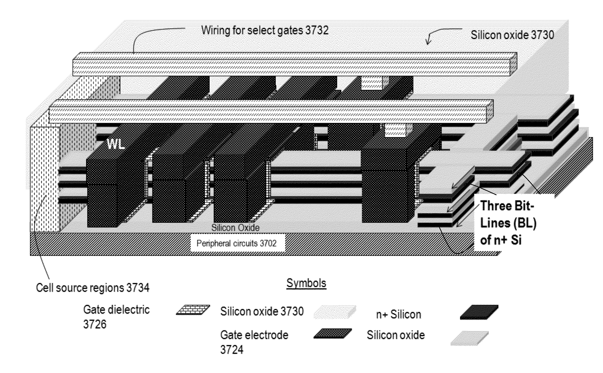
[0093]Embodiments of the present invention are now described with reference to FIGS. 1-72, it being appreciated that the figures illustrate the subject matter not to scale or to measure. Many figures describe process flows for building devices. These process flows, which are essentially a sequence of steps for building a device, have many structures, numerals and labels that are common between two or more adjacent steps. In such cases, some labels, numerals and structures used for a certain step's figure may have been described in previous steps' figures.

[0094]The thinner the transferred layer, the smaller the thru layer via diameter obtainable, due to the limitations of manufacturable via aspect ratios. Thus, the transferred layer may be, for example, less than 2 microns thick, less than 1 micron thick, less than 0.4 microns thick, less than 200 nm thick, or less than 100 nm thick. The thickness of the layer or layers transferred according to some embodiments of the present inventi...


PUM


Abstract

A semiconductor device including: a first layer including first transistors including at least one first monocrystalline silicon transistor channel; a second layer including second transistors including at least one second monocrystalline non-silicon transistor channel; a plurality of connection paths extending from the second transistors to the first transistors, where at least one of the connection paths includes at least one through layer via with a diameter of less than 200 nm.

Description

[0001]This application is a continuation of U.S. patent application Ser. No. 14 / 017,266 filed on Sep. 3, 2013, which is a continuation of U.S. patent application Ser. No. 13 / 099,010 filed on May 2, 2011, now U.S. Pat. No. 8,581,349 published on Nov. 12, 2013, which is a continuation-in-part of U.S. patent application Ser. No. 12 / 951,913 filed on Nov. 22, 2010, now U.S. Pat. No. 8,536,023 published on Sep. 17, 2013, which is a continuation-in part of U.S. patent application Ser. No. 12 / 904,119 filed on Oct. 13, 2010, now U.S. Pat. No. 8,476,145 published on Jul. 2, 2013, the entire contents all the above references are incorporated herein by reference.[0002]In addition, this application is a continuation-in part of U.S. patent application Ser. No. 13 / 016,313 filed on Jan. 28, 2011, now U.S. Pat. No. 8,362,482 published on Jan. 29, 2013, which is a continuation-in part of U.S. patent application Ser. No. 12 / 970,602 filed on Dec. 16, 2010, which is a continuation-in part of U.S. patent...

Claims


Application Information

Patent Timeline
IPC IPC(8): H01L23/538H01L27/088H01L27/06
CPCH01L23/5386H01L27/0886H01L27/0688H01L2224/16225H01L2224/32225H01L2224/73204H01L2924/15311H01L27/085H01L27/092H10B63/845H10B63/30H10N70/823H10N70/20H10N70/8833H10B12/20H10B10/125H10B41/35H10B41/20H01L2924/00H10B61/22H10N70/063H10N70/231H10N70/245H10N70/826H10N70/883
Inventor OR-BACH, ZVISEKAR, DEEPAK C.CRONQUIST, BRIAN
Owner MONOLITHIC 3D