A semiconductor device comprising a main region, a current sense region, and a well region

a semiconductor device and current sense technology, applied in the field of semiconductor devices, can solve the problems of low breakdown resistance and achieve the effect of enhancing breakdown resistan

Active Publication Date: 2015-09-10
DENSO CORP
View PDF0 Cites 5 Cited by
  • Summary
  • Abstract
  • Description
  • Claims
  • Application Information

AI Technical Summary

Benefits of technology

[0004]In the semiconductor device of Japanese Unexamined Patent Application Publication, No. 10-326897 A, the well layer formed on the outer edge of the main region and the main emitter electrode are insulated by the interlayer insulating film. For this reason, carriers flowing out of the main region into the well layer flow along the upper surface of the semiconductor substrate and easily effect current crowding in a specific location. This presents a problem of low breakdown resistance at the time of an avalanche breakdown or at the time of a short circuit.
[0006]According to the foregoing semiconductor device, the well region electrode is disposed above the well region, and the well region and the well region electrode are in contact with each other through the contact hole formed in the interlayer insulating film of the well region. For this reason, carriers flowing out of the main region into the well region quickly exit through the contact hole in the interlayer insulting film to the well region electrode. This configuration makes it hard for current crowding to be effected in the semiconductor substrate, thus making it possible to enhance breakdown resistance at the time of an avalanche breakdown or at the time of a short circuit. It should be noted that the well region electrode may be an electrode separate from the main emitter electrode, which conducts with a main emitter electrode in an external circuit, or may be an electrode formed integrally with the main emitter electrode.

Problems solved by technology

This presents a problem of low breakdown resistance at the time of an avalanche breakdown or at the time of a short circuit.

Method used


Image

  • A semiconductor device comprising a main region, a current sense region, and a well region
  • A semiconductor device comprising a main region, a current sense region, and a well region
  • A semiconductor device comprising a main region, a current sense region, and a well region

Examples


embodiment 1

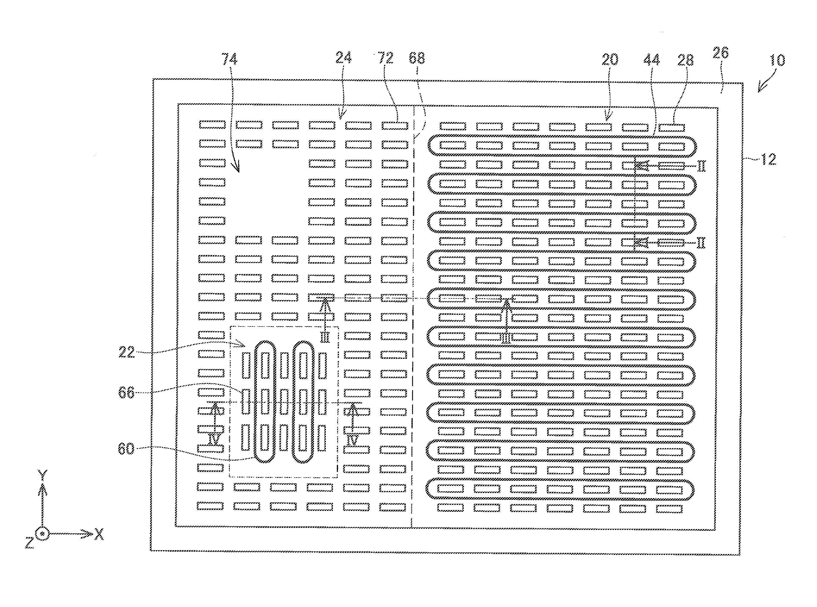
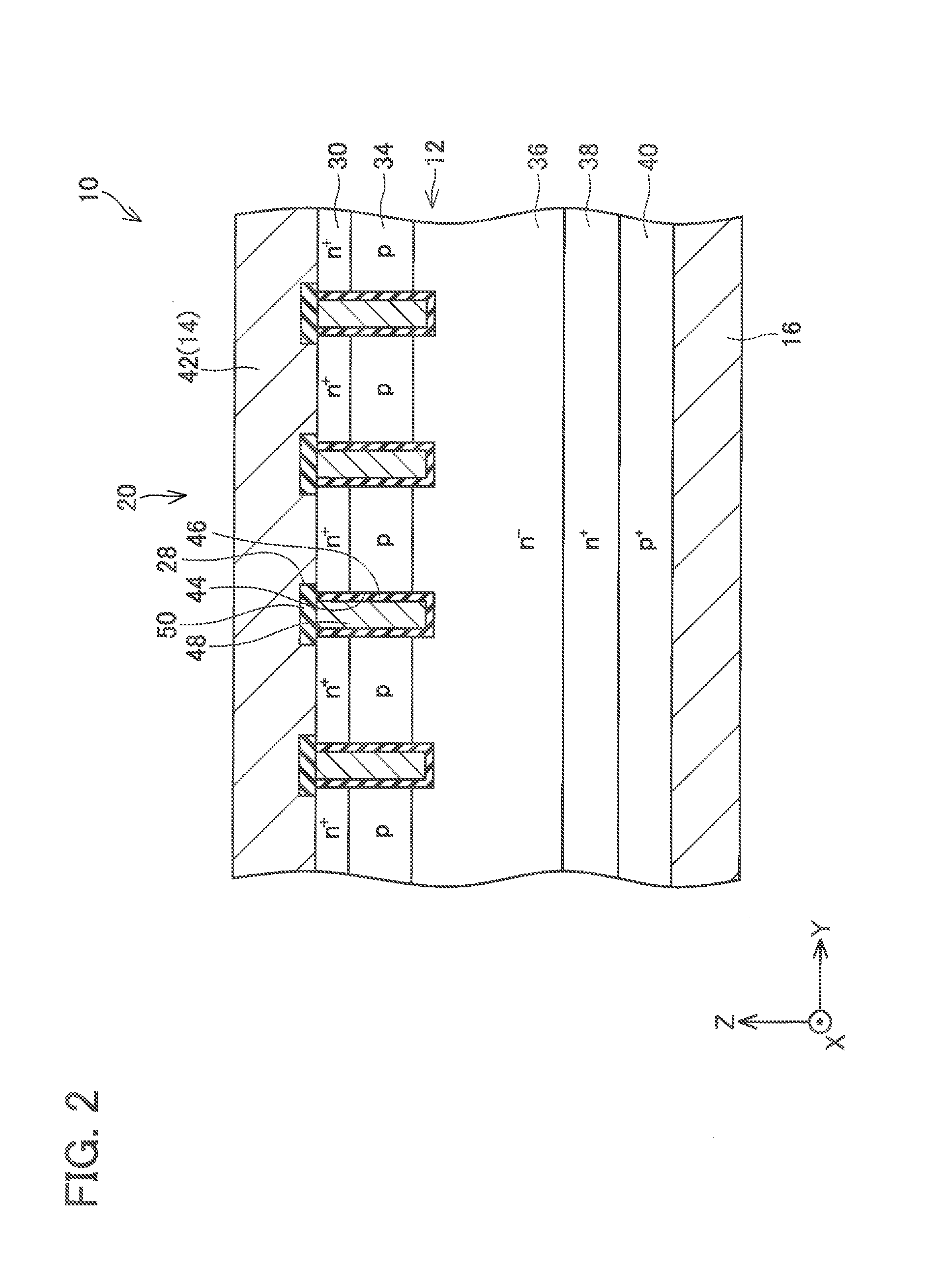
[0026]A semiconductor device 10 of the present embodiment is described below with reference to FIGS. 1 to 4. As shown in FIGS. 2 to 4, the semiconductor device 10 includes a semiconductor substrate 12, an upper electrode 14, and a lower electrode 16. The semiconductor substrate 12 is a substrate made of silicon or made of silicon carbide. The upper electrode 14 is formed on an upper surface of the semiconductor substrate 12. The lower electrode 16 is formed on a lower surface of the semiconductor substrate 12. It should be noted that for a clearer illustration, FIG. 1 omits to show the upper electrode 14.

[0027]As shown in FIG. 1, the semiconductor substrate 12 includes a main region 20, a current sense region 22, a well region 24, and a peripheral region 26. The main region 20 and the current sense region 22 both function as IGBTs. The main region 20 and the well region 24 are disposed adjacent to each other in an X direction (i.e. a left-to-right direction of FIG. 1). Further, the ...

embodiment 2

[0053]A semiconductor device 100 of the present embodiment is described below with reference to FIGS. 5 to 9. It should be noted that those components of the semiconductor device 100 of the present embodiment which are the same as those of the semiconductor device 10 of Embodiment 1 are given the same reference signs, and as such, are not described below in detail. As shown in FIGS. 6 to 9, the semiconductor device 100 includes a semiconductor substrate 102, an upper electrode 104, and a lower electrode 16. It should be noted that for a clearer illustration, FIG. 5 omits to show the upper electrode 104.

[0054]As shown in FIG. 5, the semiconductor substrate 102 includes a main region 106, a current sense region 108, a well region 110, and a peripheral region 26. The main region 106 and the current sense region 108 both function as IGBTs. The main region 106 and the well region 110 are disposed adjacent to each other in an X direction (i.e. a left-to-right direction of FIG. 5). Further...

embodiment 3

[0074]A semiconductor device 200 of the present embodiment is described below with reference to FIGS. 10 to 12. It should be noted that those components of the semiconductor device 200 of the present embodiment which are the same as those of the semiconductor device 10 of Embodiment 1 or those of the semiconductor device 100 of Embodiment 2 are given the same reference signs, and as such, are not described below in detail. As shown in FIGS. 11 and 12, the semiconductor device 200 includes a semiconductor substrate 202, an upper electrode 104, and a lower electrode 16.

[0075]As shown in FIG. 10, the semiconductor substrate 202 includes a main region 204, a current sense region 206, a well region 208, and a peripheral region 26. The main region 204 and the current sense region 206 both function as IGBTs. The main region 204 and the well region 208 are disposed adjacent to each other in an X direction (i.e. a left-to-right direction of FIG. 10). Further, the well region 208 is disposed ...


PUM


Abstract

A semiconductor device disclosed herein is configured such that a well region including a well layer is disposed between a main region of a semiconductor substrate and a current sense region of the semiconductor substrate, that a well region electrode is disposed above the well region, and that the well layer and the well region electrode are in contact with each other through a contact hole formed in an interlayer insulating film.

Description

CROSS-REFERENCE TO A RELATED APPLICATION[0001]This application claims priority to Japanese Patent Application No. 2014-041744 filed on Mar. 4, 2014, the contents of which are hereby incorporated by reference into the present application.TECHNICAL FIELD[0002]A technology disclosed herein relates to a semiconductor device.DESCRIPTION OF RELATED ART[0003]Japanese Unexamined Patent Application Publication, No. 10-326897 A discloses a semiconductor device. This semiconductor device includes: a semiconductor substrate including a main region and a current sense region; a main emitter electrode disposed above the main region of the semiconductor substrate; a current sense emitter electrode disposed above the current sense region of the semiconductor substrate; and a lower electrode disposed below the semiconductor substrate. In this semiconductor device, each of the main region and the current sense region includes: a first conductivity type emitter layer exposed at an upper surface of the...

Claims


Application Information

Patent Timeline
Patent Type & Authority Applications(United States)
IPC IPC(8): H01L29/739H01L29/423H01L29/417
CPCH01L29/7395H01L29/41708H01L29/4236H01L29/4238H01L2924/13055H01L29/66734H01L29/1095H01L29/7815H01L29/0696H01L29/404H01L29/407H01L29/7397H01L29/0619
Inventor NAGAOKA, TATSUJI
Owner DENSO CORP
Why Eureka
Try Eureka