Method of manufacturing semiconductor device

Active Publication Date: 2015-09-24
CANON KK
View PDF6 Cites 0 Cited by
  • Summary
  • Abstract
  • Description
  • Claims
  • Application Information

AI Technical Summary

Benefits of technology

The present invention provides a technique for reducing a variation in the height of an STI-type isolation insulating film in a semiconductor device. This is achieved by forming a patterned first film over a semiconductor substrate and then removing a portion of the second film located over the first film using polishing and processing techniques. This helps to reduce the difference in the height of the second film located over the first region and the second region, which may occur due to an occupancy difference between the two regions.

Problems solved by technology

When an element isolation region is formed using the STI method, this occupancy difference may lead to a variation in the height of the isolation insulating film embedded in a trench.
When there is a variation in the height of the isolation insulating film, it is difficult to contain the height of the isolation insulating film within an appropriate range.

Method used


Image

  • Method of manufacturing semiconductor device
  • Method of manufacturing semiconductor device
  • Method of manufacturing semiconductor device

Examples


Embodiment Construction

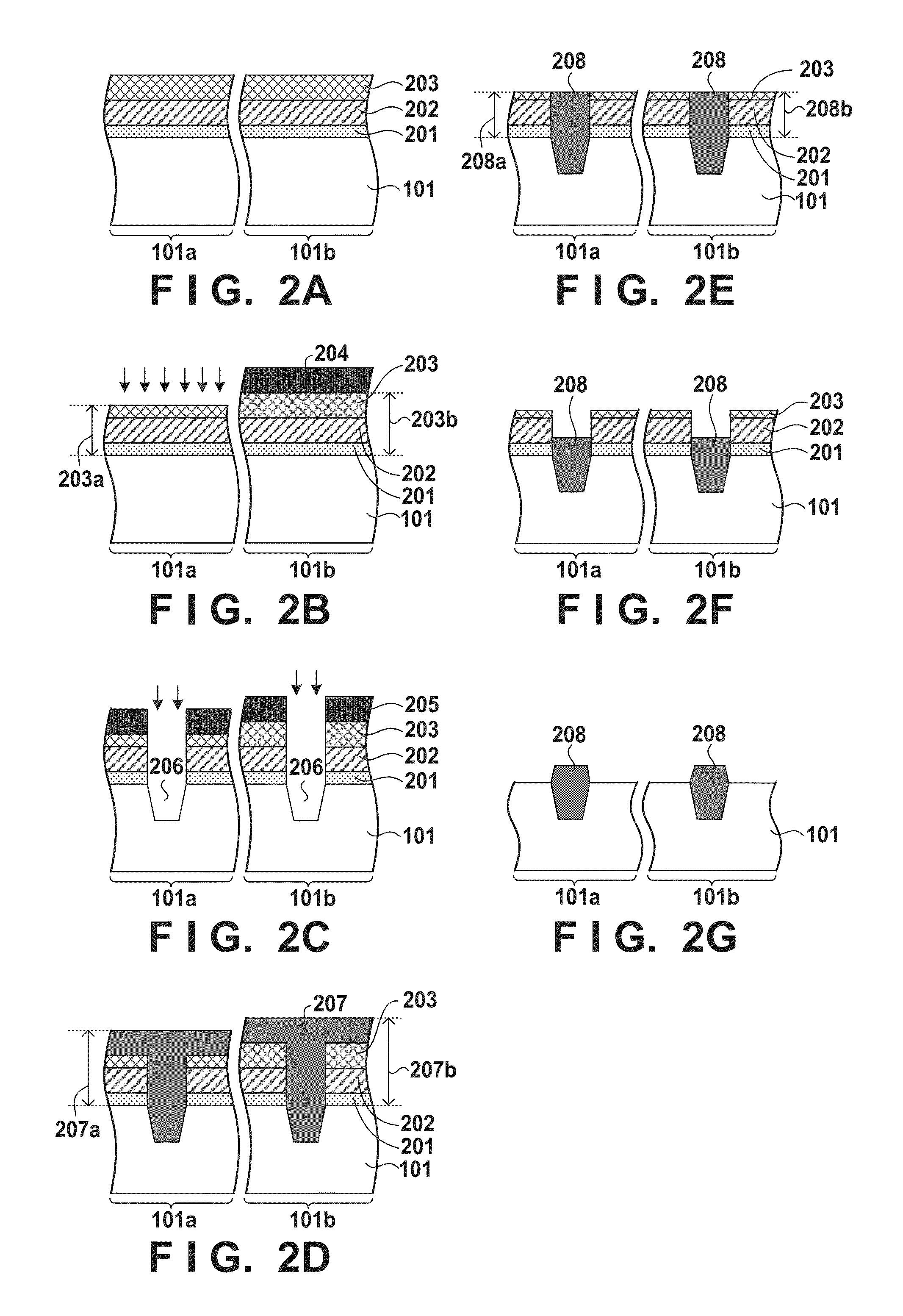
[0014]Hereinafter, embodiments of the present invention will be described with reference to the accompanying drawings. Common elements among various embodiments are assigned identical reference numerals and overlapping description will be omitted. The embodiments may be changed or combined as appropriate. The present invention is applicable to any given semiconductor device having an STI-type isolation insulating film. Hereinafter, a photoelectric conversion device will be described as an example of such a semiconductor device.

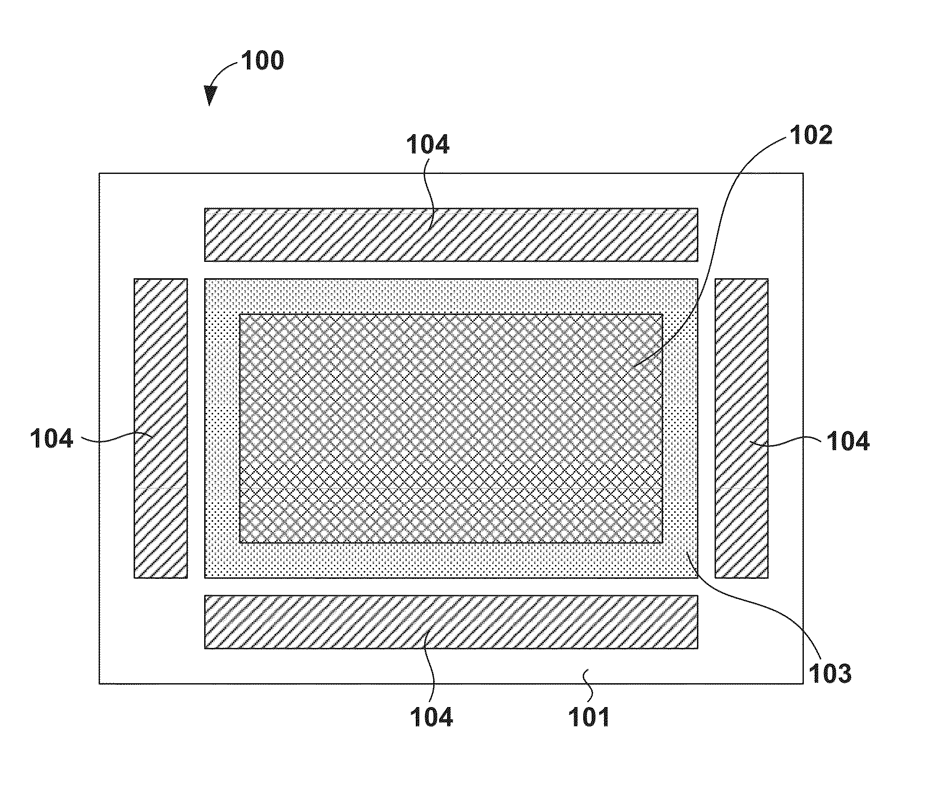
[0015]A configuration example of a photoelectric conversion device 100 according to an embodiment will be described with reference to a plan view in FIG. 1. The photoelectric conversion device 100 includes a pixel region 102 and peripheral circuit regions 104 arranged therearound provided on a semiconductor substrate 101. The semiconductor substrate 101 is formed of silicon, for example. The pixel region 102 refers to a region in which pixels including a photo...


PUM


Abstract

A method of manufacturing a semiconductor device includes forming, over a semiconductor substrate comprising a first region and a second region, a patterned first film in which an upper face of a portion located over the first region is positioned at a lower height from the semiconductor substrate than an upper face of a portion located over the second region, forming, over the first film, a second film which is an insulating film, a portion of the second film penetrating the first film and being located inside a trench of the semiconductor substrate, and polishing the second film to remove a portion of the second film located over the first film. An occupancy of the trench in the first region is lower than an occupancy of the trench in the second region.

Description

BACKGROUND OF THE INVENTION[0001]1. Field of the Invention[0002]The present invention relates to a method of manufacturing a semiconductor device.[0003]2. Description of the Related Art[0004]Photoelectric conversion regions and transistors for processing signals therefrom are being more and more miniaturized in photoelectric conversion devices (e.g., CMOS image sensors) used for digital cameras or video cameras or the like. Japanese Patent Laid-Open No. 2003-142674 forms an element isolation region using not a conventional LOCOS method but an STI method for such miniaturization.SUMMARY OF THE INVENTION[0005]With advances in the miniaturization of a pixel region in photoelectric conversion devices, an occupancy (area occupancy) of a light-receiving region in the pixel region is increasing. As a result, in the photoelectric conversion devices, an occupancy of an element isolation region in the pixel region is different from an occupancy of an element isolation region in a peripheral c...

Claims


Application Information

Patent Timeline
IPC IPC(8): H01L27/146
CPCH01L27/14685H01L21/76229H01L27/1463H01L27/14689
Inventor OKABE, TAKEHITO
Owner CANON KK
Why Eureka
Try Eureka