Active-matrix substrate, display panel and display device including the same
Active Publication Date: 2015-10-15
SHARP KK
View PDF10 Cites 73 Cited by
Summary
Abstract
Description
Claims
Application Information
AI Technical Summary
This helps you quickly interpret patents by identifying the three key elements:
Problems solved by technology
Method used
Benefits of technology
Benefits of technology
[0033]The arrangements of the present invention reduce dullness of a potential provid
Problems solved by technology
However, according to JP 2004-538511 A, the distance of routing of the gate lines is greater than in conventional devices, increasing the loa
Method used
Image
Click on the blue label to locate the original text in one second.
Reading with bidirectional positioning of images and text.
Examples
Example
First Embodiment
[0207](Construction of Liquid Crystal Display Device)
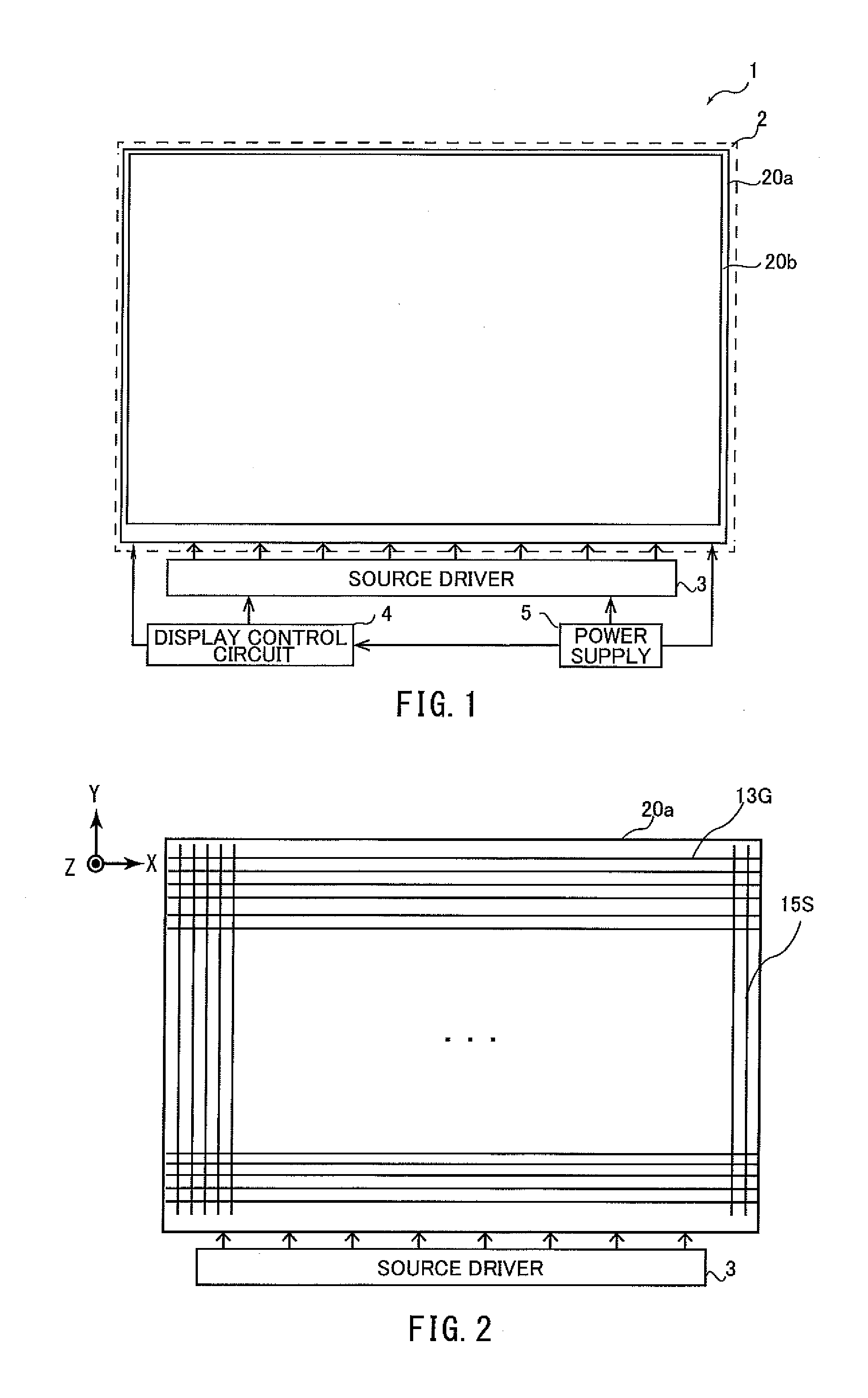
[0208]FIG. 1 is a schematic plan view of a liquid crystal display device according to the present embodiment. The liquid crystal display device 1 includes a display panel 2, a source device 3, a display control circuit 4, and a power supply 5. The display panel 2 includes an active-matrix substrate 20a, a counter-substrate 20b, and a liquid crystal layer (not shown) sandwiched between these substrates. Although not shown in FIG. 1, a polarizer is provided on the lower side of the active-matrix substrate 20a and another polarizer is provided on the upper side of the counter-substrate 20b. On the counter-substrate 20b are provided: a black matrix, red (R), green (G) and blue (B) color filters, and a common electrode (all not shown).
[0209]As shown in FIG. 1, the active-matrix substrate 20a is electrically connected with the source driver 3, which is provided on a flexible substrate. The display control circuit 4 is el...
Example
Second Embodiment
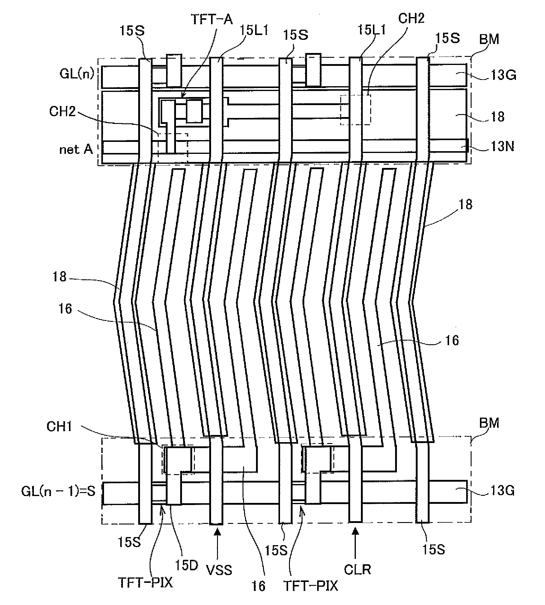
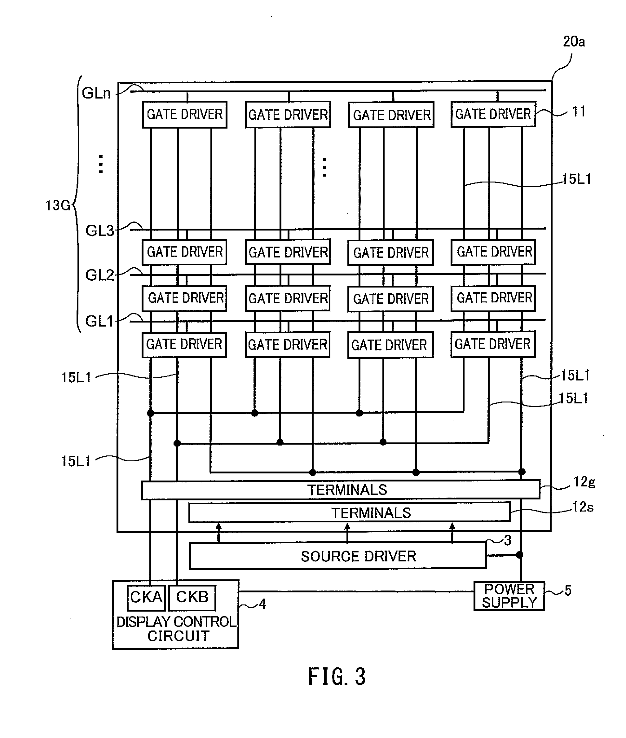
[0277]The above first embodiment describes an implementation where all the elements constituting each gate driver 11 are provided inside the display region. The present embodiment describes an implementation where some of the elements constituting each gate driver 11 are provided inside the display region. FIG. 10A is a schematic diagram showing a portion of each gate driver 11 provided inside the display region and the other portions of the gate drivers 11 provided outside the display region. As shown in FIG. 10A, in the present embodiment, in the display region 20A of the active-matrix substrate 20a are provided, in addition to the gate lines 13G and source lines 15S, TFTs-F and capacitors Cbst, lines 15L1 for supplying the TFTs-F with clock signals (CKA, CKB), and lines 13N connecting the TFTs-F and capacitors Cbst with the netA.
[0278]The portions of the gate drivers 11 except the TFTs-F and capacitors Cbst are provided in the external region 2A (i.e. outside the...
Example
Third Embodiment
[0282]The present embodiment describes a liquid crystal display device including a display panel 2 according to the first embodiment contained in a lens-integrated housing. FIG. 11 is a schematic cross-sectional view of the liquid crystal display device according to the present embodiment. As shown in FIG. 11, the liquid crystal display device 1A includes a lens-integrated housing 60 (i.e. an example of a housing), a display panel 2 and a backlight 70.
[0283]The lens-integrated housing 60 includes a housing body 60A (i.e. an example of a second cover portion) and a cover 60B (i.e. an example of a first cover portion). The housing body 60A includes a housing side 61 and a housing bottom 62. The housing side 61 is translucent and is provided on the side 2s of the display panel 2, which is parallel to the Y axis of the display panel 2 shown in FIG. 2, so as to cover the side 2s. The housing bottom 62 is provided below the backlight 70 so as to cover the bottom of the bac...
PUM
Abstract
A technique is provided that reduces dullness of a potential provided to a line such as gate line on an active-matrix substrate to enable driving the line at high speed and, at the same time, reduces the size of the picture frame region. On an active-matrix substrate (20a) are provided gate lines (13G) and source lines. On the active-matrix substrate (20a) are further provided: gate drivers (11) each including a plurality of switching elements, at least one of which is located in a pixel region, for supplying a scan signal to a gate line (13G); and lines (15L1) each for supplying a control signal to the associated gate driver (11). A control signal is supplied by a display control circuit (4) located outside the display region to the gate drivers (11) via the lines (15L1). In response to a control signal supplied, each gate driver (11) drives the gate line (13G) to which it is connected.
Description
TECHNICAL FIELD[0001]The present invention relates to an active-matrix substrate, a display panel and a display device including the same, and, more particularly, to the arrangement of gate drivers.BACKGROUND ART[0002]Display panels are known where gate drivers are provided along a side of an active-matrix substrate and source drivers are provided along an adjacent side thereof. JP 2004-538511 A discloses a technique to provide, along one side of the pixel element array, a row driving circuit for driving column address conductors for supplying data signals and a column driving circuit for driving row address conductors for supplying row selection signals. Thus, JP 2004-538511 A prevents these driving circuits from limiting the region around the pixel element array on the support body that holds the pixel element array and other components.DISCLOSURE OF THE INVENTION[0003]When a potential corresponding to a selection or non-selection state of a gate line is supplied to a gate line th...
Claims
Application Information
Patent Timeline
Application Date:The date an application was filed.
Publication Date:The date a patent or application was officially published.
First Publication Date:The earliest publication date of a patent with the same application number.
Issue Date:Publication date of the patent grant document.
PCT Entry Date:The Entry date of PCT National Phase.
Estimated Expiry Date:The statutory expiry date of a patent right according to the Patent Law, and it is the longest term of protection that the patent right can achieve without the termination of the patent right due to other reasons(Term extension factor has been taken into account ).
Invalid Date:Actual expiry date is based on effective date or publication date of legal transaction data of invalid patent.

