
Array Substrate and Display Panel

a display panel and array substrate technology, applied in the field of array substrate and display panel, can solve the problems of lowering production quality and improving the discharge speed of storage capacitance, and achieve the effects of reducing static electricity, reducing the occurrence of afterimage phenomenon, and simplifying the structure of the array substra

Active Publication Date: 2015-11-12
BOE TECH GRP CO LTD +1
View PDF16 Cites 17 Cited by
  • Summary
  • Abstract
  • Description
  • Claims
  • Application Information

AI Technical Summary

Benefits of technology

The invention aims to improve the speed of discharging storage capacitance in a display panel, which can reduce afterimage phenomenon. It includes an array substrate with a discharge unit that selectively connects data lines to common electrode lines for fast discharging. Additionally, an electrostatic protection unit and a test unit are connected to the same switching signal line, simplifying the structure of the array substrate and reducing static electricity on the data line while enabling test of the liquid crystal screen.

Problems solved by technology

However, with the improvement of display resolution, since the speed of discharge of the storage capacitance corresponding to the pixel electrode is limited, afterimage phenomenon may occur in the process of switching two image frames, thus the production quality is lowered.
Therefore, how to improve the speed of discharge of the storage capacitance corresponding to the pixel electrode becomes a technical problem required to be solved urgently in the art.

Method used


Image

  • Array Substrate and Display Panel
  • Array Substrate and Display Panel
  • Array Substrate and Display Panel

Examples


Embodiment Construction

[0028]The specific implementations of the present invention are described below in detail with conjunction with the accompanying drawings. It should be understood that the specific implementations described herein are merely used for describing and explaining the present invention, rather than limiting the present invention.

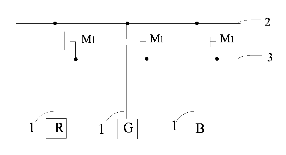
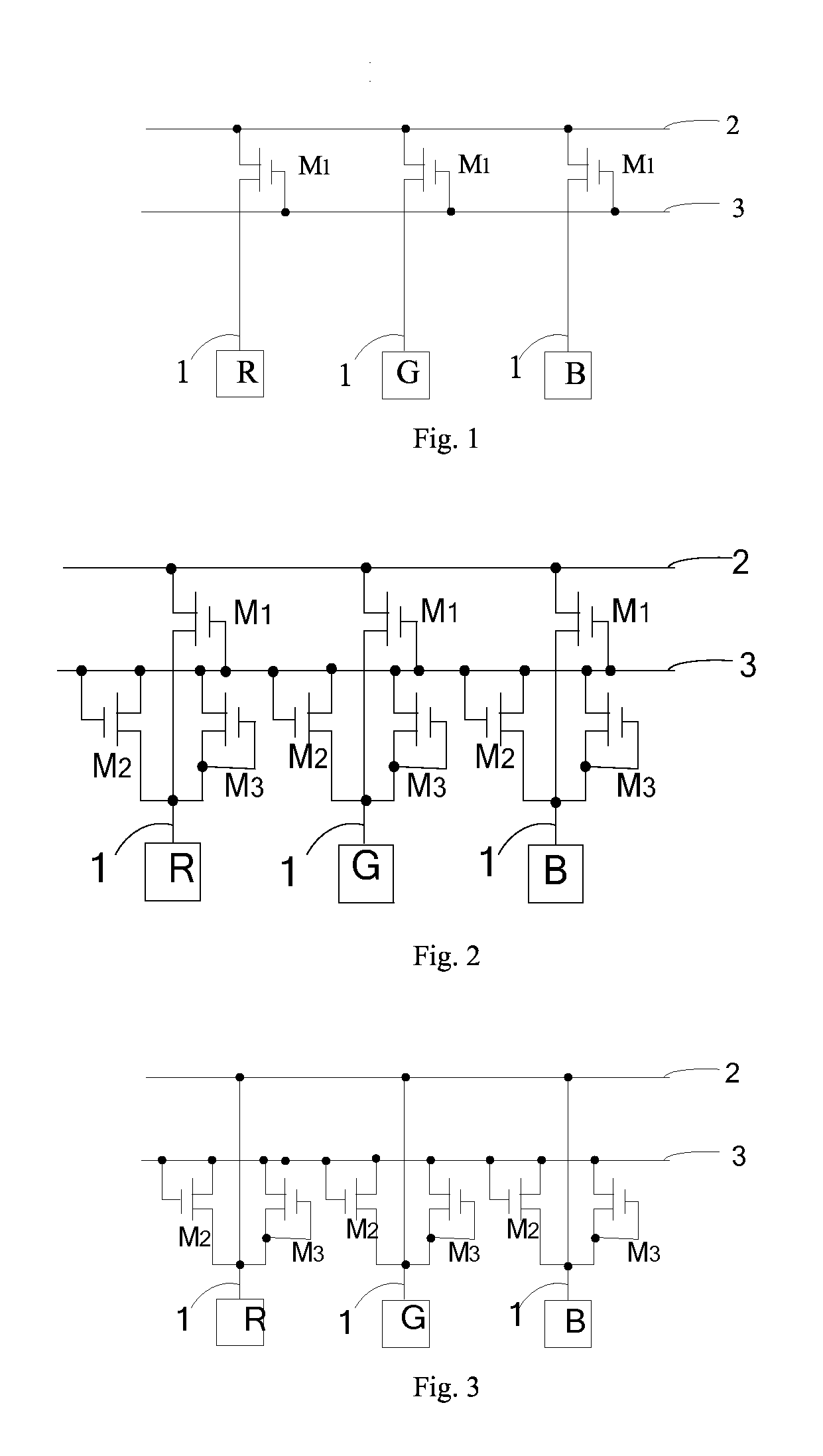
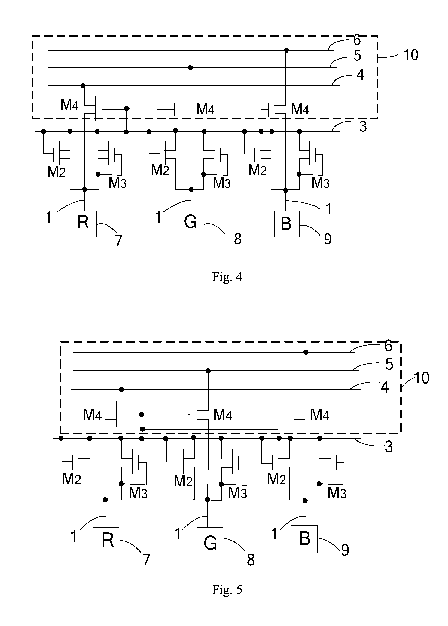
[0029]The present invention provides an array substrate comprising a plurality of data lines 1 and a plurality of common electrode lines 2, the array substrate further comprises at least one discharge unit, each discharge unit corresponds to one of the plurality of data lines 1, and is connected between the corresponding data line 1 and one of the plurality of common electrode lines 2, and each discharge unit can selectively conduct the data line 1 to the common electrode line 2 connected thereto.

[0030]Since at least one discharge unit is provided, the discharge unit can selectively conduct the data line 1 connected thereto to the common electrode line 2 connecte...


PUM


Abstract

The present invention provides an array substrate and a display panel. The array substrate comprises a plurality of data lines and a plurality of common electrode lines, wherein, the array substrate further comprises at least one discharge unit, each discharge unit corresponds to one of the plurality of data lines and is connected between the corresponding data line and one of the plurality of common electrode lines, and each discharge unit can selectively conduct the data line to the common electrode line connected thereto. The display panel comprises the array substrate. In the present invention, the discharge unit can selectively conduct the data line connected thereto to the common electrode line connected thereto, to enable fast discharge of the storage capacitance and reduce occurrence of afterimage phenomenon.

Description

FIELD OF THE INVENTION[0001]The present invention relates to the field of liquid crystal display technology, and particularly to an array substrate and a display panel.BACKGROUND OF THE INVENTION[0002]Thin Film transistor liquid crystal display (TFT-LCD), due to its high image quality, low power consumption, low cost and the like, has been widely used after decades of development.[0003]In the working process of a liquid crystal display, when the liquid crystal liquid displays an image, a thin film transistor corresponding to a pixel electrode is turned on, a signal may be transmitted to the pixel electrode through a data line, that is, storage capacitance formed by the pixel electrode and a common electrode is charged; when the liquid crystal display does not display an image (i.e., at a time interval between two image frames), the storage capacitance formed by the pixel electrode and the common electrode discharges. However, with the improvement of display resolution, since the spe...

Claims


Application Information

Patent Timeline
IPC IPC(8): G09G3/36
CPCG09G3/3648G09G2300/0478G09G2300/0426G09G2300/0404G02F1/136204G02F1/136286G02F1/136254
Inventor WEI, XIANGDONGHAO, XUEGUANGLI, CHENGAN, SEONGJUNRYU, BONGYEOL
Owner BOE TECH GRP CO LTD
Learn More