Vertical transistor and method to form vertical transistor contact node

a technology of vertical transistors and contact nodes, which is applied in the direction of basic electric elements, electrical equipment, semiconductor devices, etc., can solve the problem that the contact node does not have an ideal low contact resistance, and achieve the effect of reducing the outward contact resistance of the gate structur

Active Publication Date: 2015-12-03
MICRON TECH INC
View PDF6 Cites 0 Cited by
  • Summary
  • Abstract
  • Description
  • Claims
  • Application Information

AI Technical Summary

Benefits of technology

[0008]The present invention, therefore, discloses a vertical transistor structure and a method for forming contact node of the vertical transistor structure. In order to solve the problem of contact resistance when simply using silicon as a electrical contact node, the present invention particularly proposes a composite contact node in the vertical transistor structure, which can reduce the outward contact resistance of the gate structure in the vertical transistor structure.

Problems solved by technology

However, the current process simply uses silicon as a material for the node, so the contact node does not have an ideal low contact resistance (outward contact resistance), which has become one obstacle to the performance improvement of the dynamic random access memory.

Method used


Image

  • Vertical transistor and method to form vertical transistor contact node
  • Vertical transistor and method to form vertical transistor contact node
  • Vertical transistor and method to form vertical transistor contact node

Examples


Embodiment Construction

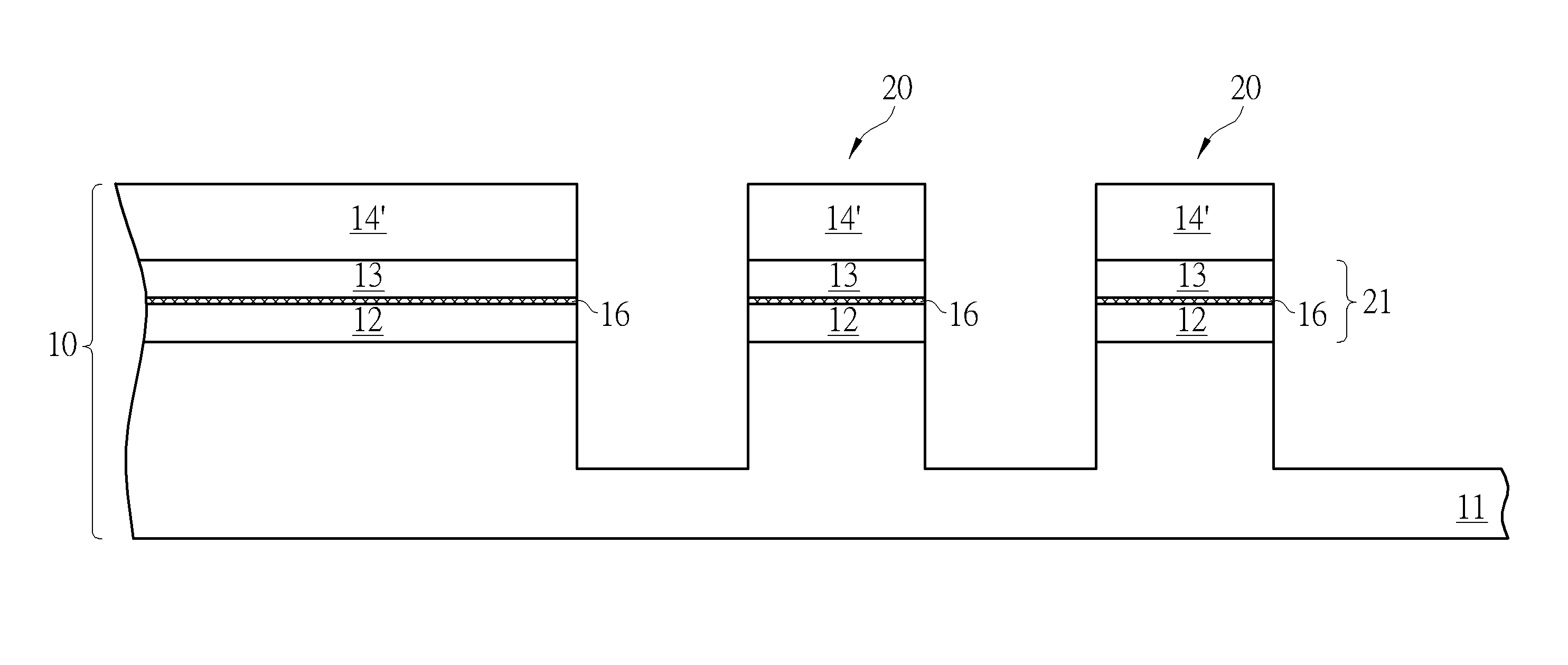
[0043]The present invention provides a vertical transistor structure having a composite contact node and a method for forming such composite contact node in the vertical transistor structure. To address the problem of unsatisfactory contact resistance because only silicon material is typically used as an electrical contact node, the present invention provides a composite contact node in the vertical transistor structure. The proposed composite contact node can reduce the outward contact resistance of a gate structure of the vertical transistor structure. Further, the conductive material used in the composite contact node can help to form a landing pad with the lower electrode of the other elements.

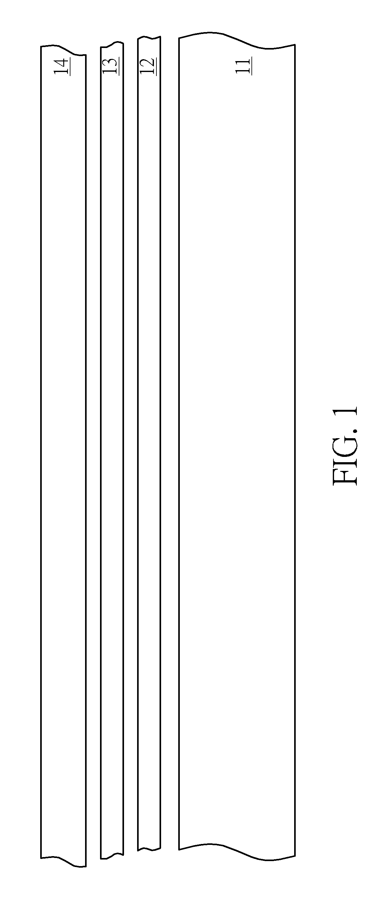
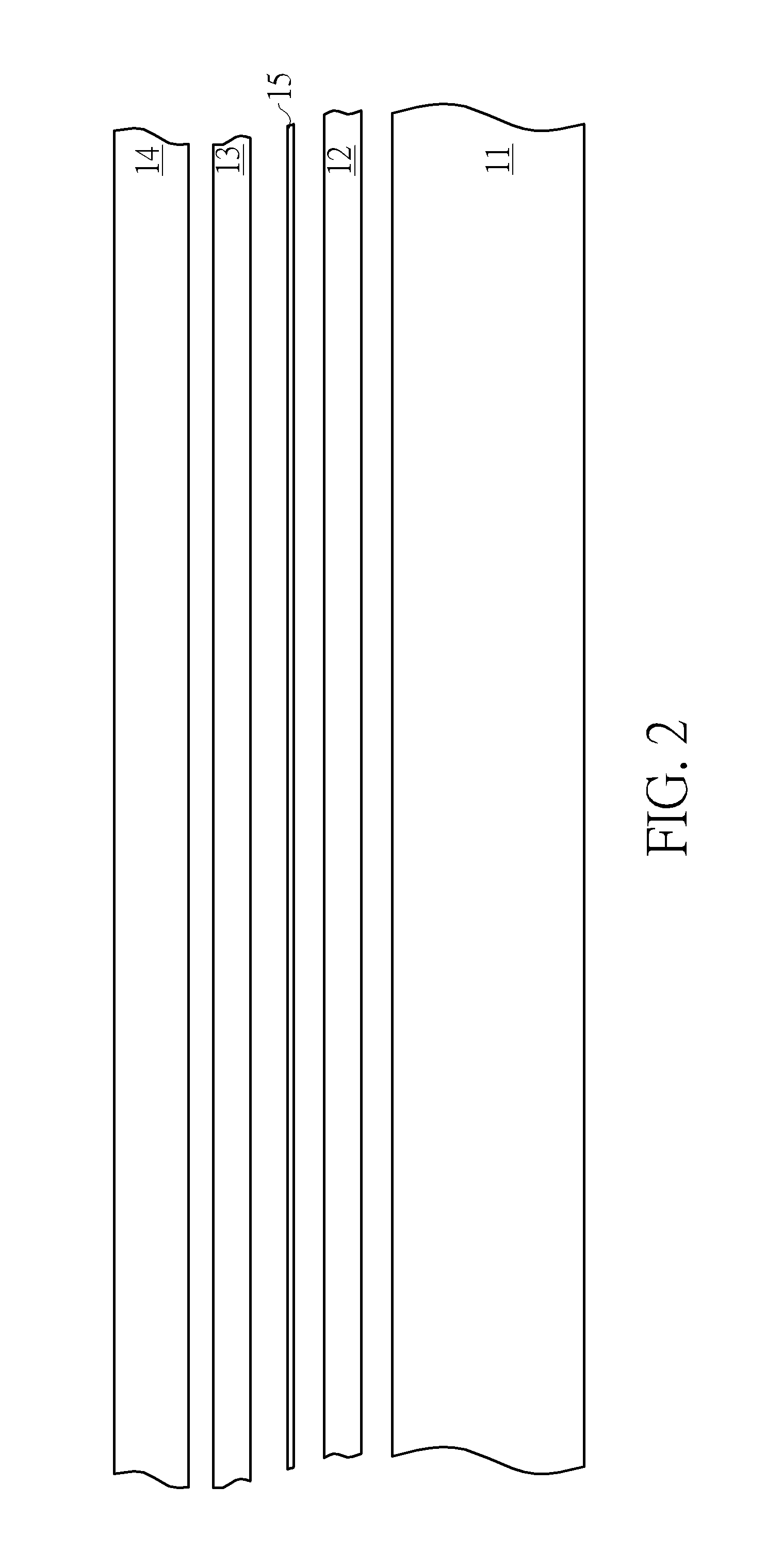
[0044]According to one aspect of the present invention, a method for forming a contact node of a vertical transistor structure is provided. Referring to FIG. 3, a laminated material layer 10 is prepared. The laminated material layer 10 comprises a substrate 11, a buffer layer (offset layer...


PUM


Abstract

A vertical transistor structure includes a substrate with a protruding structure, an offset layer covering a top surface of the protruding structure, a conductive layer disposed on the offset layer, and an interlayer disposed between the offset layer and the conductive layer to serve as a contact node.

Description

CROSS REFERENCE TO RELATED APPLICATION[0001]This application claims the benefit of Taiwan patent application No. 103118454, filed on May 27, 2014, the disclosure of which is incorporated herein in its entirety by reference.BACKGROUND OF THE INVENTION[0002]1. Field of the Invention[0003]The present invention generally relates to a vertical transistor structure and a method of forming a contact node of the vertical transistor structure. In particular, the present invention for forming a composite contact node in the vertical transistor structure, whereby the outward contact resistance of the vertical transistor structure can be reduced.[0004]2. Description of the Prior Art[0005]Dynamic random access memory (DRAM) is a semiconductor element wherein a capacitor structure is electrically connected to a gate structure. The storage capacitor is the core elements of the dynamic random access memory, which is responsible for storing the signal or data. Depending on the position of the storag...

Claims


Application Information

Patent Timeline
Patent Type & Authority Applications(United States)
IPC IPC(8): H01L29/78H01L29/66
CPCH01L29/7827H01L29/665H01L29/66666H01L29/66553
Inventor LEE, TZUNG-HAN
Owner MICRON TECH INC
Why Eureka
Try Eureka