Light absorption film, preparation method and application

a light absorption film and film technology, applied in vacuum evaporation coating, optical elements, instruments, etc., can solve the problems of easy degradation of paint, inability to wear-resistant, complicated procedures for etching and laser processing, etc., to achieve simple and convenient preparation, cost-effective effect, and large area

Pending Publication Date: 2021-10-28
NINGBO INST OF MATERIALS TECH & ENG CHINESE ACADEMY OF SCI
View PDF3 Cites 2 Cited by
  • Summary
  • Abstract
  • Description
  • Claims
  • Application Information

AI Technical Summary

Benefits of technology

The present patent describes a light absorption film that has a wide frequency range for light absorption, a high absorption rate, and stable physical and chemical properties. The film has a layered structure and a conical surface structure that allows for multiple reflections of incident light, resulting in sufficient absorption. The film can be coated on different substrates and has a controllable structure and stable physical and chemical properties. Additionally, a method for preparing the film is provided that is cost-effective, simple, and can realize a large-area preparation.

Problems solved by technology

A light absorption layer can be produced on the surface of a material by brushing black paint, electrochemical etching and laser processing, but each has its own disadvantage: the paint is prone to degradation and is not wear-resistant, and the etching and laser processing are complicated in procedure.

Method used


Image

  • Light absorption film, preparation method and application
  • Light absorption film, preparation method and application
  • Light absorption film, preparation method and application

Examples


example 1 preparation

of Light Absorption Film

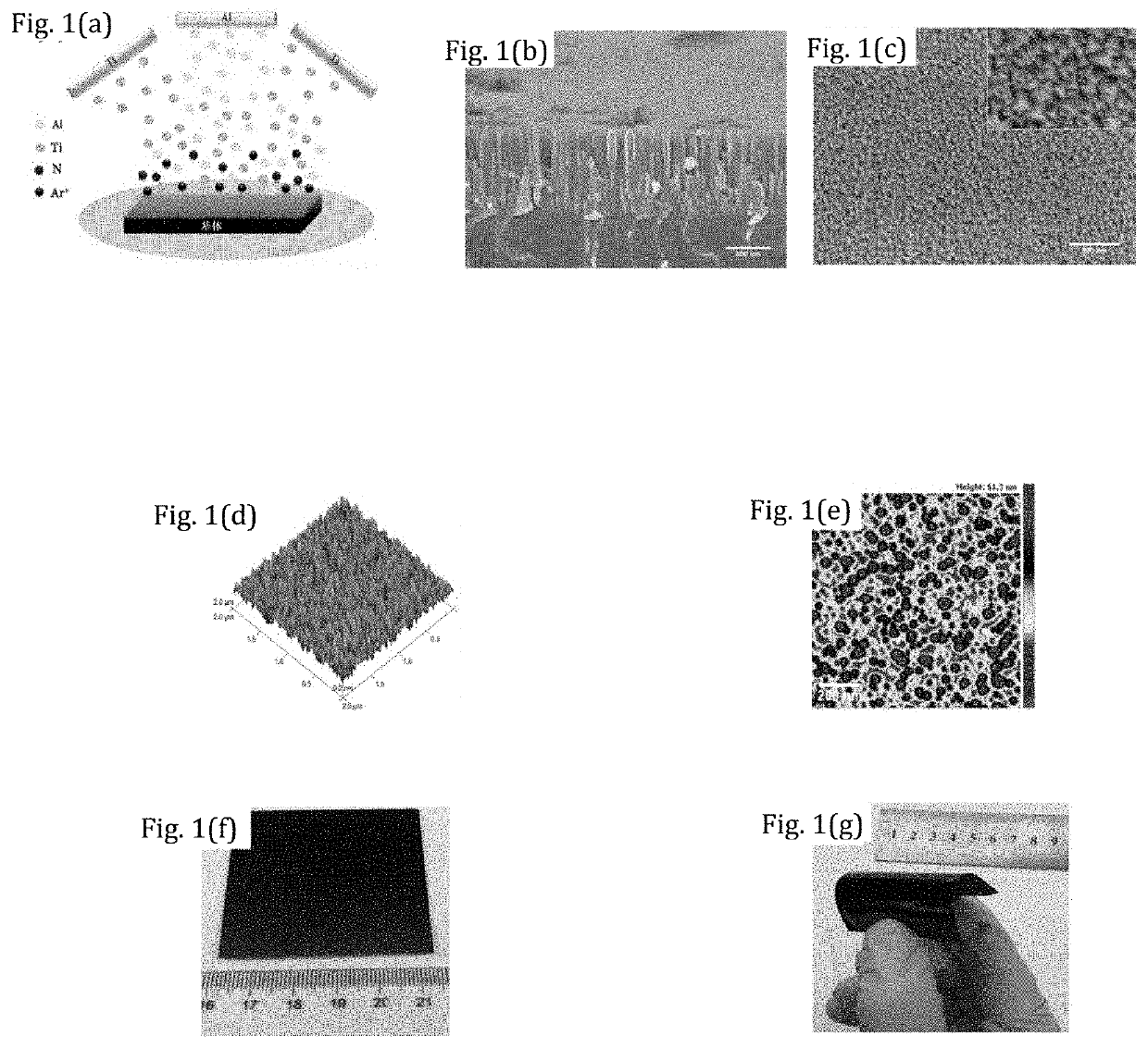
[0075]A vacuum apparatus equipped with two or more magnetron sputtering targets was used, wherein the targets were respectively a high-purity titanium target and a high-purity aluminum target with a purity of 99.999%, and the sizes of the targets were: titanium target: Φ100 mm×10 mm, and aluminum target: Φ100 mm×20 mm. The two sputtering targets were connected to two direct current power sources, respectively. The two targets were each inclined by 15° to direct to the coating area together. The distance between the targets and the substrate was 10 cm.

[0076]In order to ensure the cleanness of the sample surface, the substrate might be subjected to ultrasonic and absolute alcohol washing before being coated.

[0077]Preparation of Sample 1#

[0078]Copper was used as the substrate, and the copper substrate was placed in the coating area. The vacuum degree of the vacuum apparatus was applied to 7.0×10⁻⁴ Pa, and high-purity argon gas of 99.999% was introduced at a flow...

example 2

Structure Characterization of Light Absorption Film

[0092]Sample 1# was used as a typical sample, the cross-sectional morphology was characterized by the scanning electron microscopy. As shown in FIG. 1(b) and FIG. 1(c), a columnar crystal structure is clearly observed in FIG. 1(b), and the crystal grains have a width of 30˜50 nm and a thickness of 800˜900 nm, wherein the columnar crystal structures with a crystal grain width of around 50 nm and a thickness of around 900 nm account for a relatively large proportion of around 70%-90%.

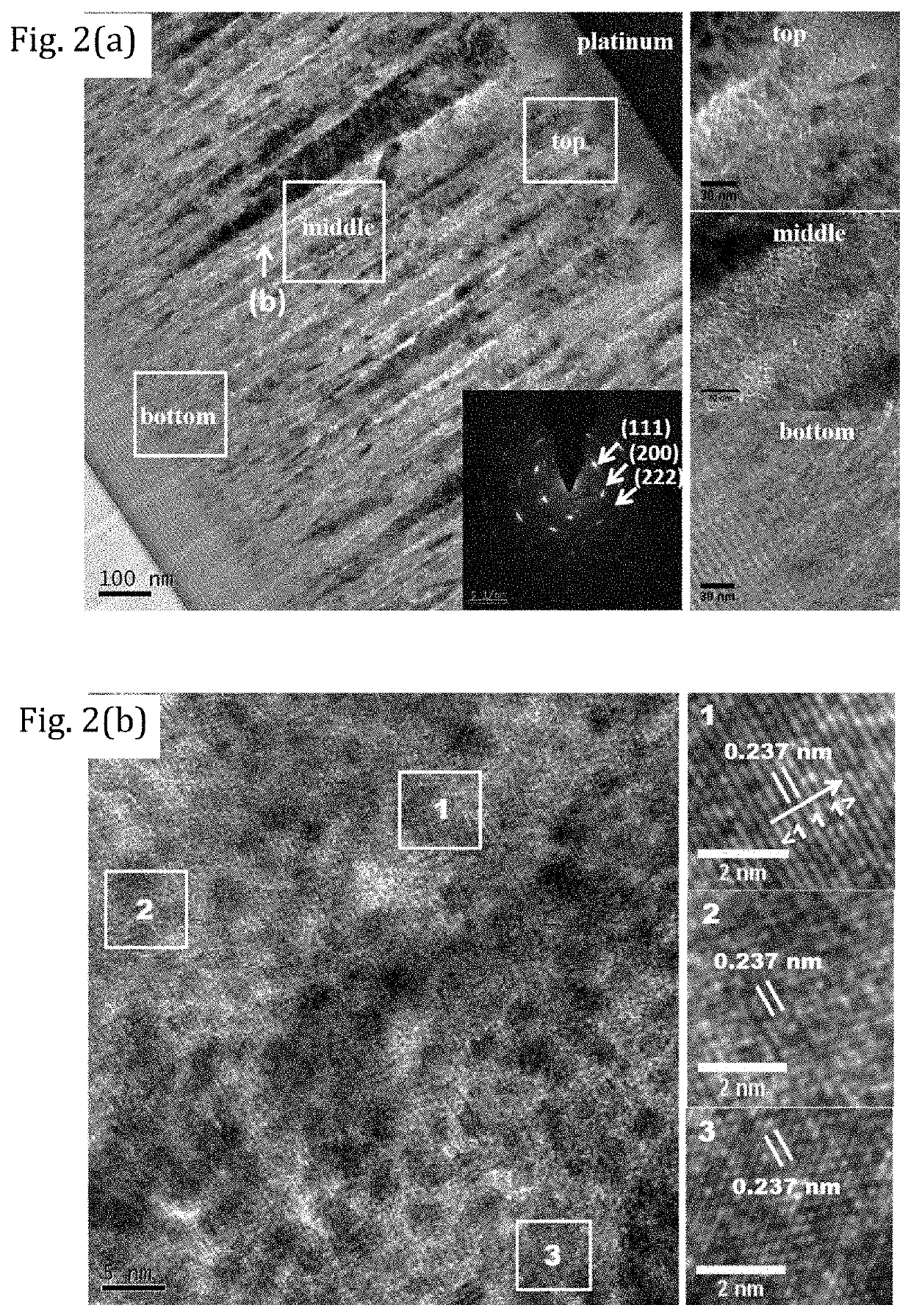
[0093]The structure of sample 1# was characterized by the transmission electron microscope. As shown in FIG. 2, a nano-layered structure on the bottom of the sample and an outer columnar crystal structure can be observed in FIG. 2(a), wherein the columnar crystals have a crystal grain width of around 50 nm and a height of around 900 nm; a subboundary structure inside the columnar crystals can be observed in FIG. 2(b), wherein the width of the subboundary ...

example 3 performance

Characterization of Light Absorption Film

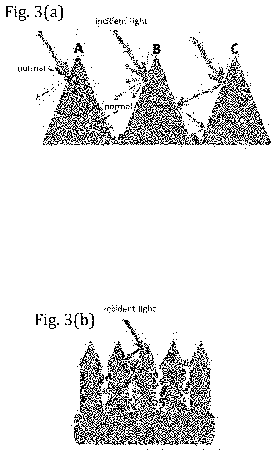
[0105]FIG. 3 is a schematic diagram showing the light absorption mechanism of the light absorption film in the present application, wherein (a) is a schematic diagram showing the process of incident light being entered from the surface of the film into the interior of the film, and (b) is a schematic diagram showing the process of light being reflected repeatedly between the grain boundaries to increase absorption.

[0106]The reflection rates of total reflection, diffuse reflection and specular reflection of sample 1# were determined, as shown in FIG. 4(a). It can be seen from the figure that in the total reflection, the intensity of the specular reflection is extremely low, and the light absorption rate is enhanced, indicating that the light absorption performance of the film prepared is good enough.

[0107]The light absorption performances of samples 6#, 7# and 8# were tested, as shown in FIG. 4(b). It can be seen from the figure that the light...


PUM

PropertyMeasurementUnit
light wavelengthaaaaaaaaaa
thicknessaaaaaaaaaa
thicknessaaaaaaaaaa

Abstract

A light absorption film. The light absorption film is a titanium-aluminum-nitride film, including a bottom layer and an outer layer; the bottom layer has a nano-layered structure, the outer layer has a columnar crystal structure, and the top of the columnar crystal structure is a conical surface; within a light wavelength range of 200 nm to 2500 nm, the light absorption film has an average light absorption rate (α) of not less than 0.89. After adding an antireflection layer of TiAlON, TiO2 or SiO2 to the outer layer of the light absorption film, the average light absorption rate (α) is not less than 0.95 within the light wavelength range of 200 nm to 2500 nm. The light absorption film has advantages of such as a wide frequency range for light absorption, a high absorption rate, and stable physical and chemical properties of the film in adverse environments.

Description

TECHNICAL FIELD[0001]The present application refers to a light absorption film, preparation method and application, belonging to the fields of materials and physical vapor deposition.BACKGROUND[0002]A high-performance light absorption film can be widely applied in solar thermal conversion, heat management, internal extinction of optical instruments and so on. A light absorption layer can be produced on the surface of a material by brushing black paint, electrochemical etching and laser processing, but each has its own disadvantage: the paint is prone to degradation and is not wear-resistant, and the etching and laser processing are complicated in procedure. Ti-based coating prepared by magnetron sputtering system is a currently common method for industrial production of light absorption films, which has good light absorption performances within a certain range of spectrum. However, for full-band light absorption, a three-dimensional structure is usually further required.[0003]Theref...

Claims


Application Information

Patent Timeline
Patent Type & Authority Applications(United States)
IPC IPC(8): G02B5/00C23C14/35C23C14/34C23C14/06C23C14/08C23C14/10
CPCG02B5/003C23C14/352C23C14/3464G02B1/113C23C14/0676C23C14/083C23C14/10C23C14/0641C23C14/0036C23C14/3414C23C16/34G02B5/208G02B1/118B82Y20/00
Inventor SONG, ZHENLUNWATTOO, ABDUL GHAFARDING, XUEFENGYANG, LIJINGZHENG, BICHANGJIANG, JIANJUNHU, FANGQIN
Owner NINGBO INST OF MATERIALS TECH & ENG CHINESE ACADEMY OF SCI
Why Eureka
Try Eureka