Method for preparing unary or binary patterning colloidal photonic crystal
A colloidal photonic crystal and patterning technology, applied in chemical instruments and methods, crystal growth, single crystal growth, etc., can solve the problems of complex preparation process, limited application range, high cost, etc., and achieve simple operation and broad application prospects , the effect of uniform thickness and orientation
- Summary
- Abstract
- Description
- Claims
- Application Information
AI Technical Summary
Problems solved by technology
Method used
Image
Examples
Embodiment 1
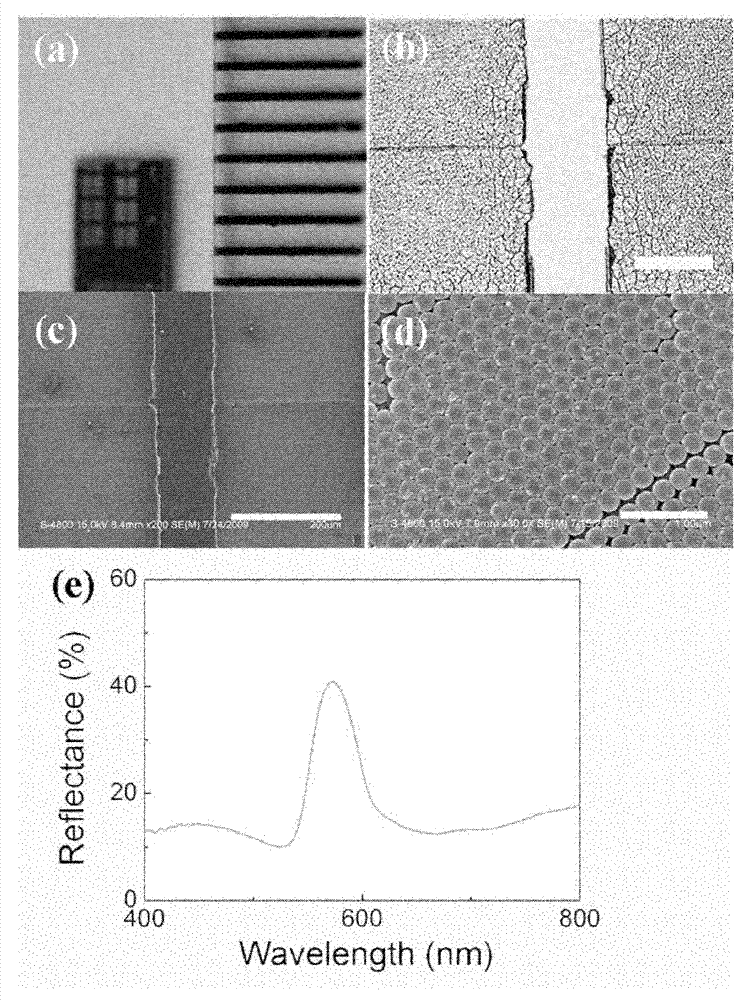
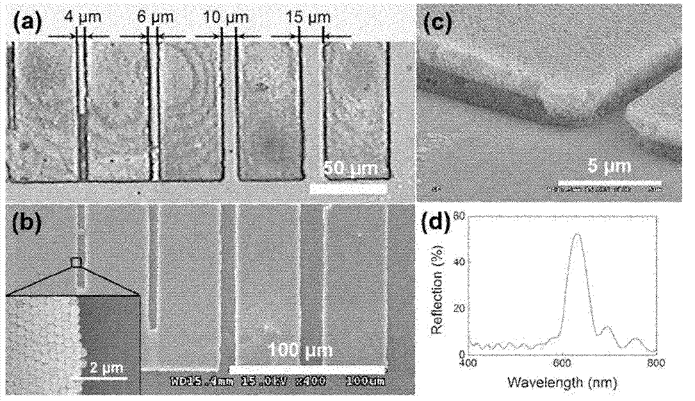
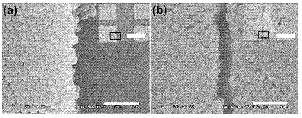
[0029] 1) Spin-coat a layer of photoresist with a thickness of 2 microns on a clean and hydrophilic silicon substrate. After etching, obtain patterned substrate, on this patterned substrate, use vacuum evaporation method (vacuum degree is 10 -3 Pa) prepare one deck thickness to be the chromium layer of 2 nanometers, on the chromium layer, use vacuum evaporation method again (vacuum tightness is 10 -3 Pa) After preparing a layer of copper layer with a thickness of 20 nanometers, the substrate is inserted into an aqueous dispersion containing monodisperse 250nm polystyrene microspheres (the volume percentage of polystyrene microspheres is 0.1%, and the degree of dispersion is 3 %) at a constant temperature of 65°C to obtain a unitary patterned colloidal photonic crystal film with a thickness of 2 microns on the surface of the substrate;
[0030] 2) Soak the substrate obtained in step 1) in an ethanol solvent for 10 minutes, and then ultrasonicate for 2 seconds at an ultrasonic ...
Embodiment 2
[0033] 1) Spin-coat a layer of photoresist with a thickness of 2 microns on a clean and hydrophilic silicon substrate. After etching, obtain patterned substrate, on this patterned substrate, use vacuum evaporation method (vacuum degree is 10 -3 Pa) prepare one deck thickness to be the chromium layer of 2 nanometers, on the chromium layer, use vacuum evaporation method again (vacuum tightness is 10 -3 Pa) After preparing a layer of copper layer with a thickness of 20 nanometers, the substrate is inserted into an aqueous dispersion containing monodisperse 290nm silica microspheres (the volume percentage of silica microspheres is 0.1%, and the degree of dispersion is 5 %) at a constant temperature of 65°C to obtain a unitary patterned colloidal photonic crystal film with a thickness of 2 microns on the surface of the substrate;
[0034] 2) Soak the substrate obtained in step 1) in an acetone solvent for 10 minutes, and then ultrasonicate for 2 seconds at an ultrasonic power of 2...
Embodiment 3
[0037] 1) Spin-coat a layer of photoresist with a thickness of 2 microns on a clean and hydrophilic glass substrate. After etching, obtain patterned substrate, on this patterned substrate, use vacuum evaporation method (vacuum degree is 10 -3 Pa) prepare one deck thickness to be the chromium layer of 2 nanometers, on the chromium layer, use vacuum evaporation method again (vacuum tightness is 10 -3 Pa) After preparing a layer of copper layer with a thickness of 20 nanometers, insert the substrate into an aqueous dispersion containing monodisperse 280nm silica microspheres (the volume percentage of silica microspheres is 0.1%, and the degree of dispersion is 2 %) at a constant temperature of 65°C to obtain a unitary patterned colloidal photonic crystal film with a thickness of 2 microns on the surface of the substrate;
[0038] 2) The monolithic patterned colloidal photonic crystal film obtained in step 1) is subjected to vapor deposition (vacuum degree of 3000Pa, deposition t...
PUM
| Property | Measurement | Unit |
|---|---|---|
| thickness | aaaaa | aaaaa |
| thickness | aaaaa | aaaaa |
| particle diameter | aaaaa | aaaaa |
Abstract
Description
Claims
Application Information


