Light receiving element

Active Publication Date: 2016-01-21
MITSUBISHI ELECTRIC CORP
View PDF0 Cites 3 Cited by
  • Summary
  • Abstract
  • Description
  • Claims
  • Application Information

AI Technical Summary

Benefits of technology

[0006]The present invention has been achieved to solve the above-described problems, and an object of the present invention is to provide a light

Problems solved by technology

With the light receiving element disclosed in Japanese Patent Laid-Open No. 2010-45417, there is a problem that if the thickn

Method used


Image

  • Light receiving element
  • Light receiving element
  • Light receiving element

Examples


Example

First Embodiment

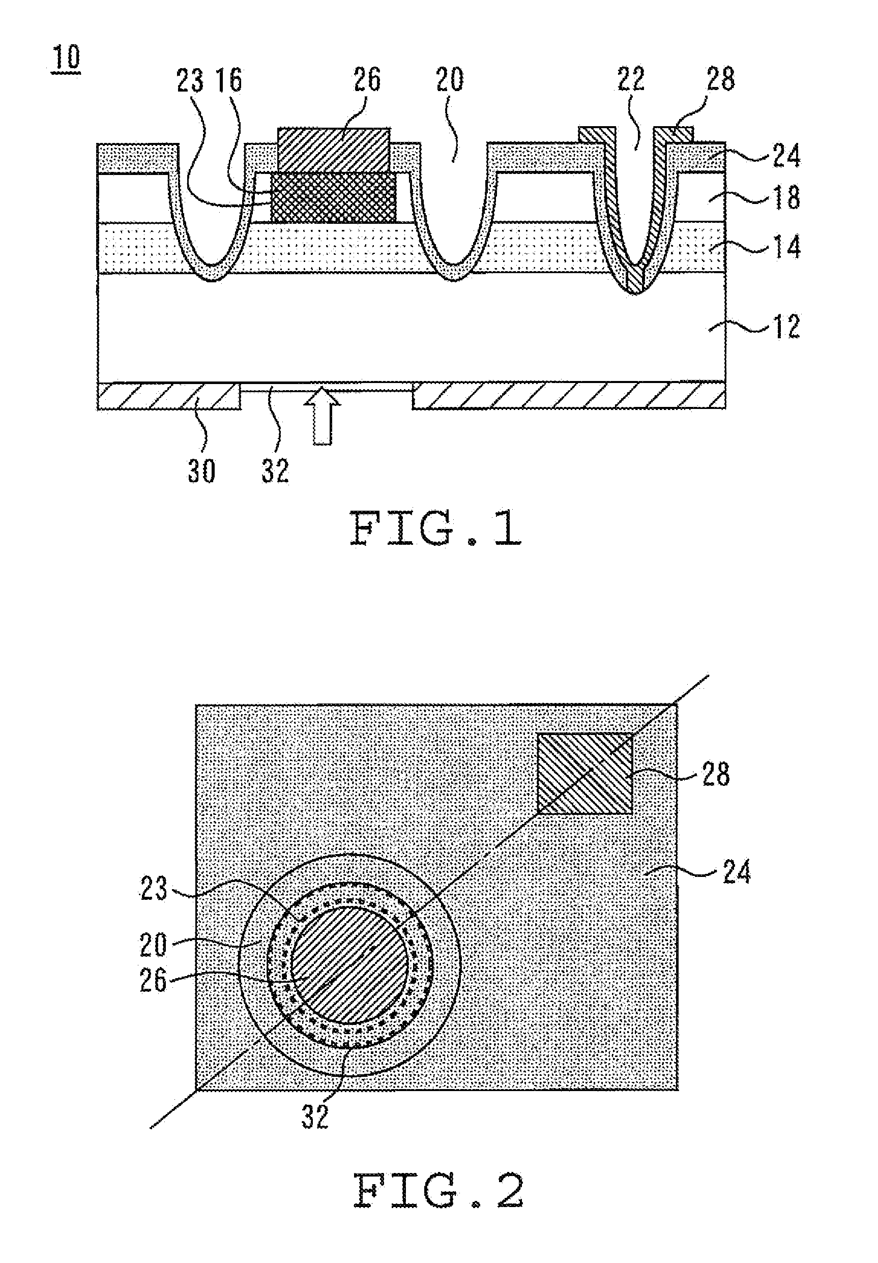
[0017]FIG. 1 is a sectional view of a light receiving element 10 according to a first embodiment of the present invention. The light receiving element 10 has a substrate 12 of a first conduction type. The substrate 12 is, for example, n-type InP. A light absorbing layer 14 of the first conduction type is formed on the substrate 12. The light absorbing layer 14 has a bandgap smaller than that of the substrate 12. The light absorbing layer 14 is, for example, n-type InGaAs.

[0018]A diffusion layer 16 of a second conduction type is formed on a portion of the light absorbing layer 14. The diffusion layer 16 is, for example, p-type InP. A window layer 18 of the first conduction type is formed on the light absorbing layer 14. The window layer 18 is formed so as to surround the diffusion layer 16 as viewed in plan. The window layer 18 has a bandgap larger than that of the light absorbing layer 14. The window layer 18 is, for example, n-type InP.

[0019]Grooves 20 and 22 are f...

Example

Second Embodiment

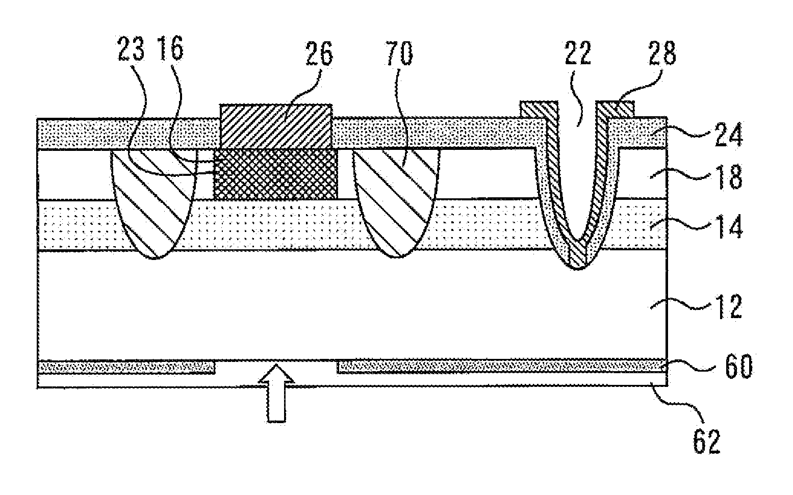
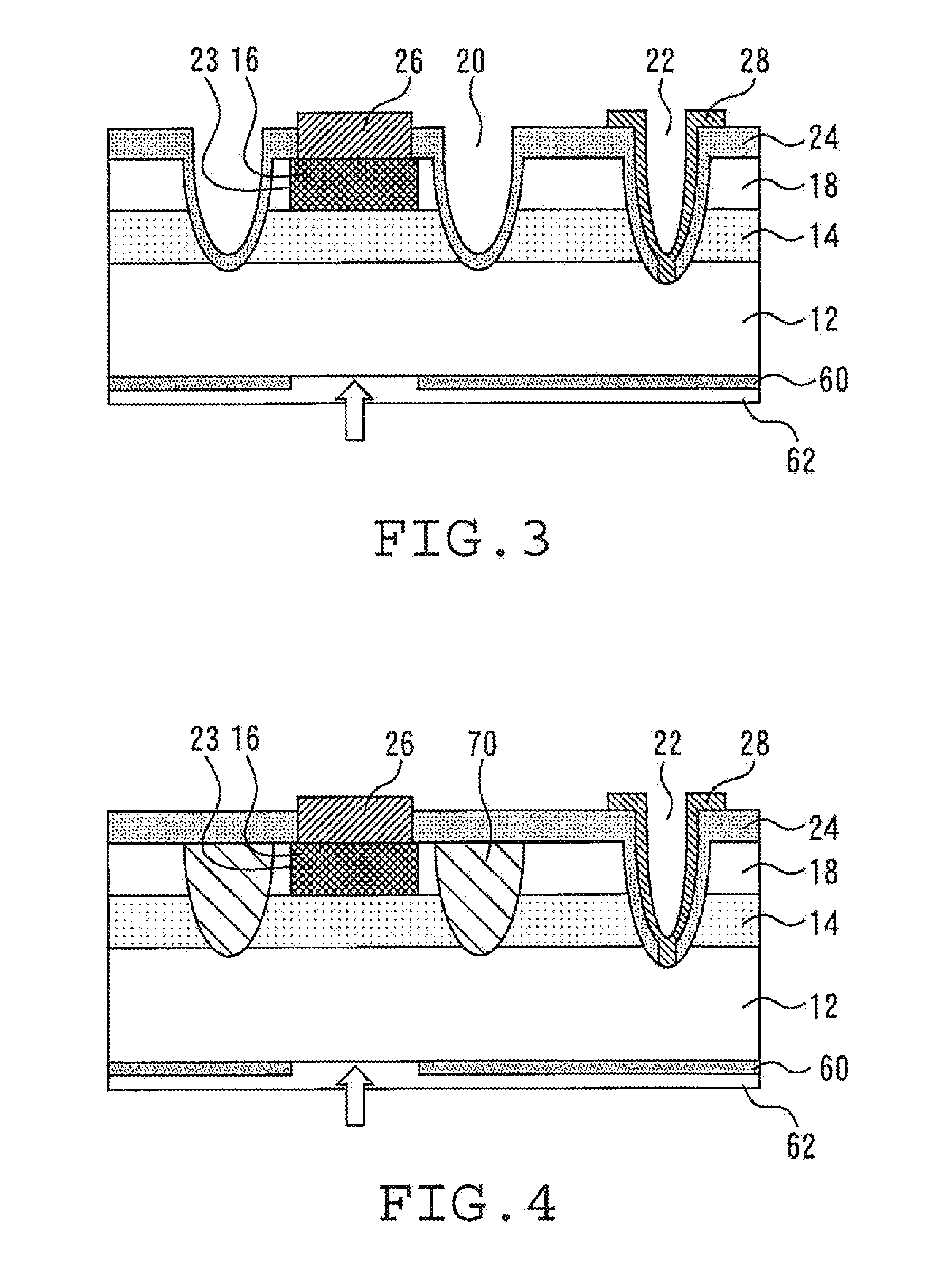
[0032]FIG. 3 is a sectional view of a light receiving element according to a second embodiment of the present invention. A portion of the lower surface of the substrate 12 is covered with an epitaxial layer 60. The material of the epitaxial layer 60 is not particularly limited as long as it is capable of absorbing light. However, the material of the epitaxial layer 60 is, for example, n-type InGaAs. The epitaxial layer 60 has an opening right below the diffusion layer 16. A low-reflection film 62 is formed in this opening.

[0033]The metal mask 30 in the first embodiment reflects light and there is a possibility of the reflected light interfering with the incident light. However, in the second embodiment of the present invention, such reflection of light can be prevented since the epitaxial layer 60 capable of absorbing light is formed.

Example

Third Embodiment

[0034]FIG. 4 is a sectional view of a light receiving element according to a third embodiment of the present invention. This light receiving element is provided with an ion-implanted portion 70 formed, for example, by implantation with Ti and the like. The ion-implanted portion 70 surrounds the boundary between the diffusion layer 16 and the window layer 18 as viewed in plan, and extends through the window layer 18 and the light absorbing layer 14 as viewed in section. When light enters the ion-implanted portion 70, no carriers are generated. Also, the ion-implanted portion 70 shuts off the flow of carriers. FIG. 5 is a plan view of the light receiving element shown in FIG. 4. The ion-implanted portion 70 indicated by a broken line surrounds the boundary 23 between the diffusion layer and the window layer as viewed in plan.

[0035]The ion-implanted portion 70 has the same function as that of the groove 20 in the first embodiment. In addition, the ion-implanted portion ...


PUM


Abstract

A light receiving element includes a substrate of a first conduction type, a light absorbing layer of the first conduction type formed on the substrate, a diffusion layer of a second conduction type formed on a portion of the light absorbing layer, a window layer of the first conduction type formed on the light absorbing layer so as to surround the diffusion layer and having a bandgap larger than that of the light absorbing layer, an anode electrode formed on the diffusion layer, and a cathode electrode provided on the substrate so as to contact the substrate without contacting each of the window layer and the light absorbing layer, wherein a groove is formed which surrounds a boundary between the diffusion layer and the window layer as viewed in plan and extends through the window layer and the light absorbing layer as viewed in section.

Description

BACKGROUND OF THE INVENTION[0001]1. Field of the Invention[0002]The present invention relates to a light receiving element for use in optical communication for example.[0003]2. Background Art[0004]Japanese Patent Laid-Open No. 2010-45417 discloses a light receiving element having an anode electrode on the upper surface side of a substrate, and a cathode electrode on a lower surface of the substrate. Japanese Patent Laid-Open No. 2007-88496 discloses a light receiving element having an anode electrode and a cathode electrode on the upper surface side of a substrate.[0005]Increasing the response speed of a light receiving element requires eliminating a “current component delayed in response” which is a current component generated after a lapse of a certain time period from a time at which light enters the light receiving element. With the light receiving element disclosed in Japanese Patent Laid-Open No. 2010-45417, there is a problem that if the thickness of the substrate is increase...

Claims


Application Information

Patent Timeline
IPC IPC(8): H01L31/0224H01L31/0216
CPCH01L31/02164H01L31/022408H01L31/035281H01L31/10H01L31/02161H01L31/109
Inventor KIKUCHI, MATOBUNAKAJI, MASAHARUTAKEMURA, RYOTAYAMAJI, KAZUKI
Owner MITSUBISHI ELECTRIC CORP
Why Eureka
Try Eureka