

Semiconductor device and electronic apparatus
a technology of electromagnetic field and electronic apparatus, applied in the direction of radio frequency controlled devices, television system scanning details, television system, etc., can solve the problems of high membrane stress, large power consumption, and unsatisfactory demand, and achieve good light collection characteristics, and stress-free
Active Publication Date: 2016-01-28
SONY CORP
View PDF3 Cites 8 Cited by
- Summary
- Abstract
- Description
- Claims
- Application Information
AI Technical Summary
Benefits of technology
The patent text describes how to create an image sensor that is stressed evenly and does not have any wrinkles or distortion. This sensor also collects light very well.
Problems solved by technology
It is difficult to design a two-dimensional layout of interconnection, which leads to large power consumption.
Such a demand is becoming unsatisfied with a conventional structure in which a solid-state image sensor is provided in a ceramic package and a glass plate is attached to a surface so that the solid-state image sensor is sealed.
When the microlens is formed of SiN, which is transparent and has a high refractive index, SiN has a tendency to cause high membrane stress.
Therefore, a problem arises that a defective surface such as a blemish or distortion occurs due to a significant difference in membrane stress between the microlens and the underlying resin.
Method used
View moreImage
Smart ImageViewing Examples

Examples
first embodiment
[0042]2. Configuration of semiconductor package in first embodiment
second embodiment
[0043]3. Configuration of semiconductor package in second embodiment
third embodiment
[0044]4. Configuration of semiconductor package in third embodiment
Login to View More PUM
 Abstract
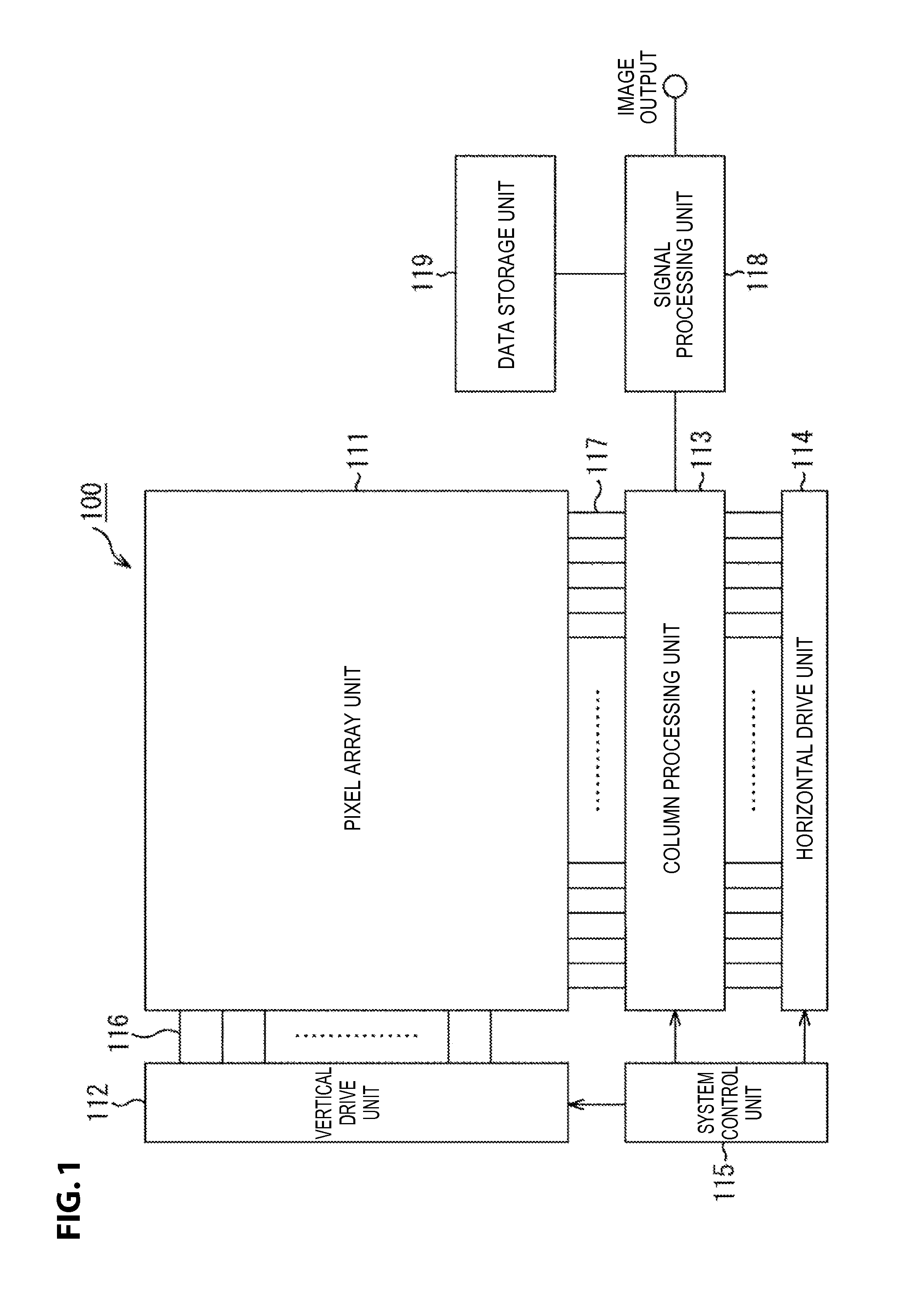
Provided is a semiconductor device including: a multilayer substrate including an optical element; a light-transmitting plate provided on the substrate to cover the optical element; and a lens of an inorganic material provided between the substrate and the light-transmitting plate. A structure having a same strength as a strength per unit area of the lens is provided at a portion outside an effective photosensitive region where the optical element is formed, when the substrate is viewed in plan.
Description
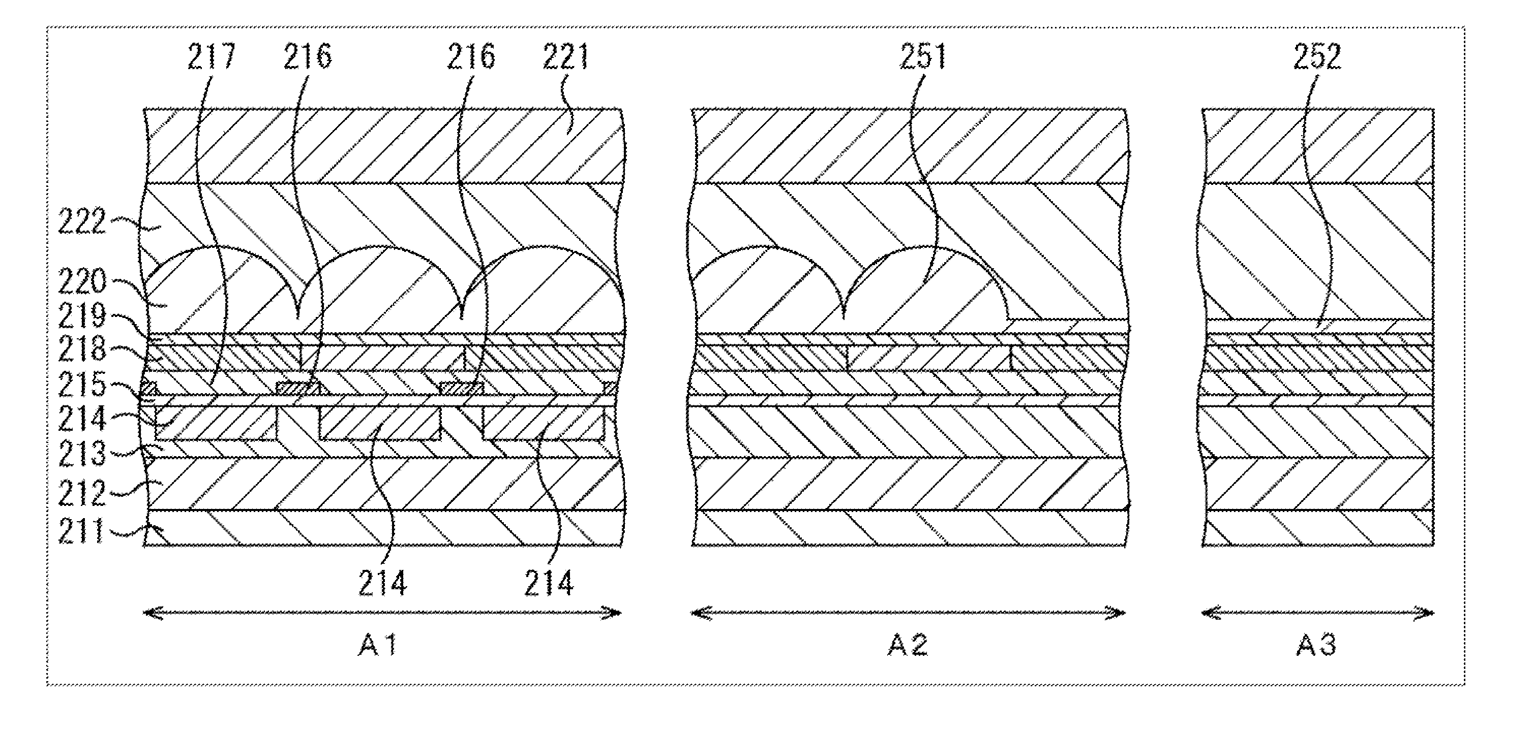
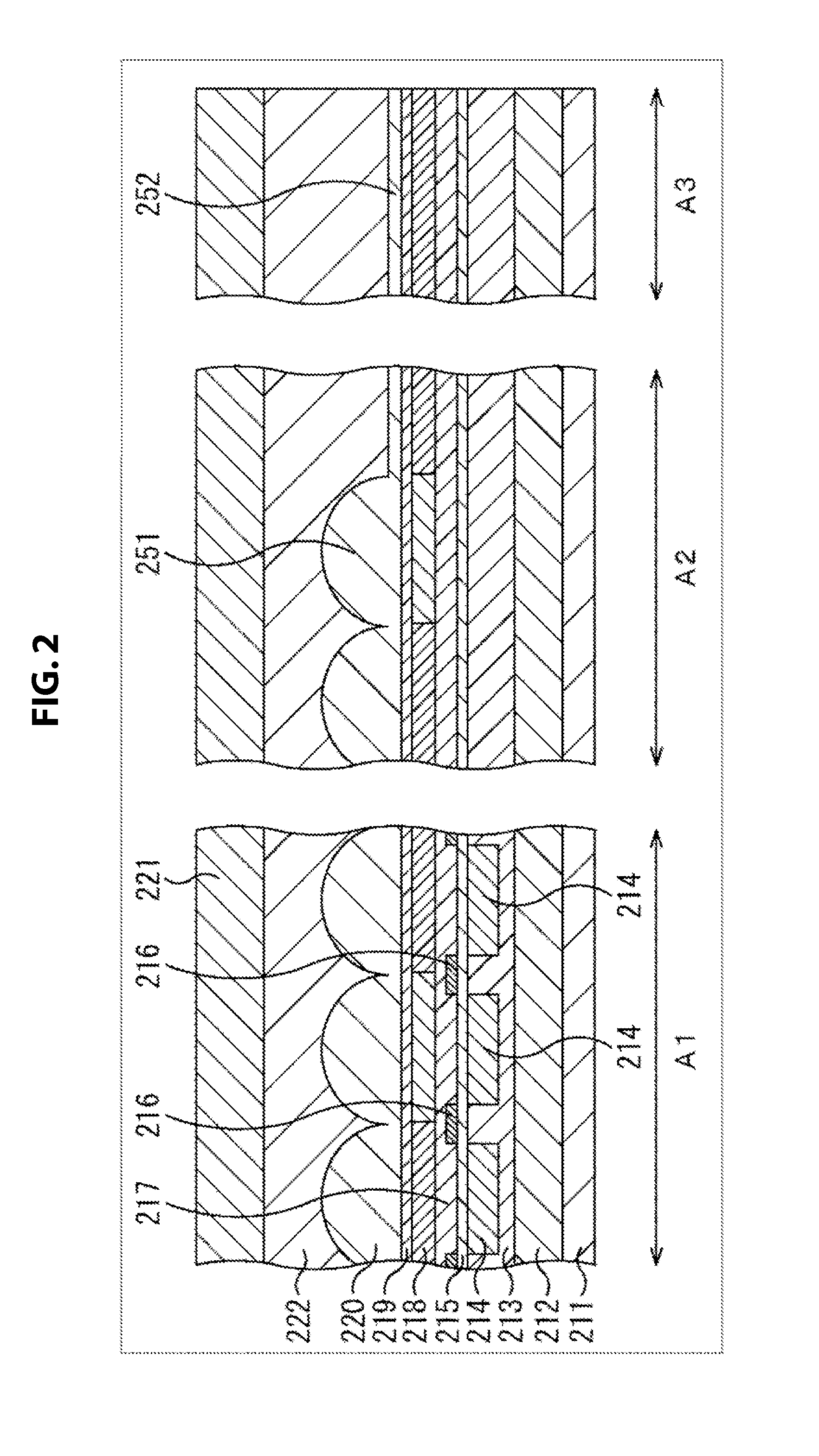
TECHNICAL FIELD [0001]The present technology relates to semiconductor devices and electronic apparatuses. More particularly, the present technology relates to a semiconductor device and electronic apparatus in which deformation of a lens does not occur.BACKGROUND ART [0002]In the recent development of semiconductor technologies, the three-dimensional multilayer technique of stacking elements in the vertical direction to construct three-dimensional structure has attracted attention as a Beyond-Moore technique that is an alternative to More-Moore techniques of increasing integration densities. It is difficult to design a two-dimensional layout of interconnection, which leads to large power consumption. It has been proposed that a three-dimensional interconnection layout in which circuit blocks having various functions are divided into multiple layers, and chips are connected together, can reduce power consumption or increase processing speed. It has also been proposed that the use of ...
Claims
Login to View More Application Information
Patent Timeline
 Patent Type & AuthorityApplications(United States)
IPC IPC(8): H01L27/146H04N5/374
CPCH01L27/14627H04N5/374H01L27/14618H01L27/1464H01L27/14623H01L27/14685H04N25/76H01L27/14621H01L27/14636
InventorHIRANO, TAKAAKIMIYAZAWA, SHINJIMAEDA, KENSAKUMORIYA, YUSUKEFURUSE, SHUNSUKEOOKA, YUTAKA
OwnerSONY CORP