Semiconductor device including semiconductor chips stacked over substrate
- Summary
- Abstract
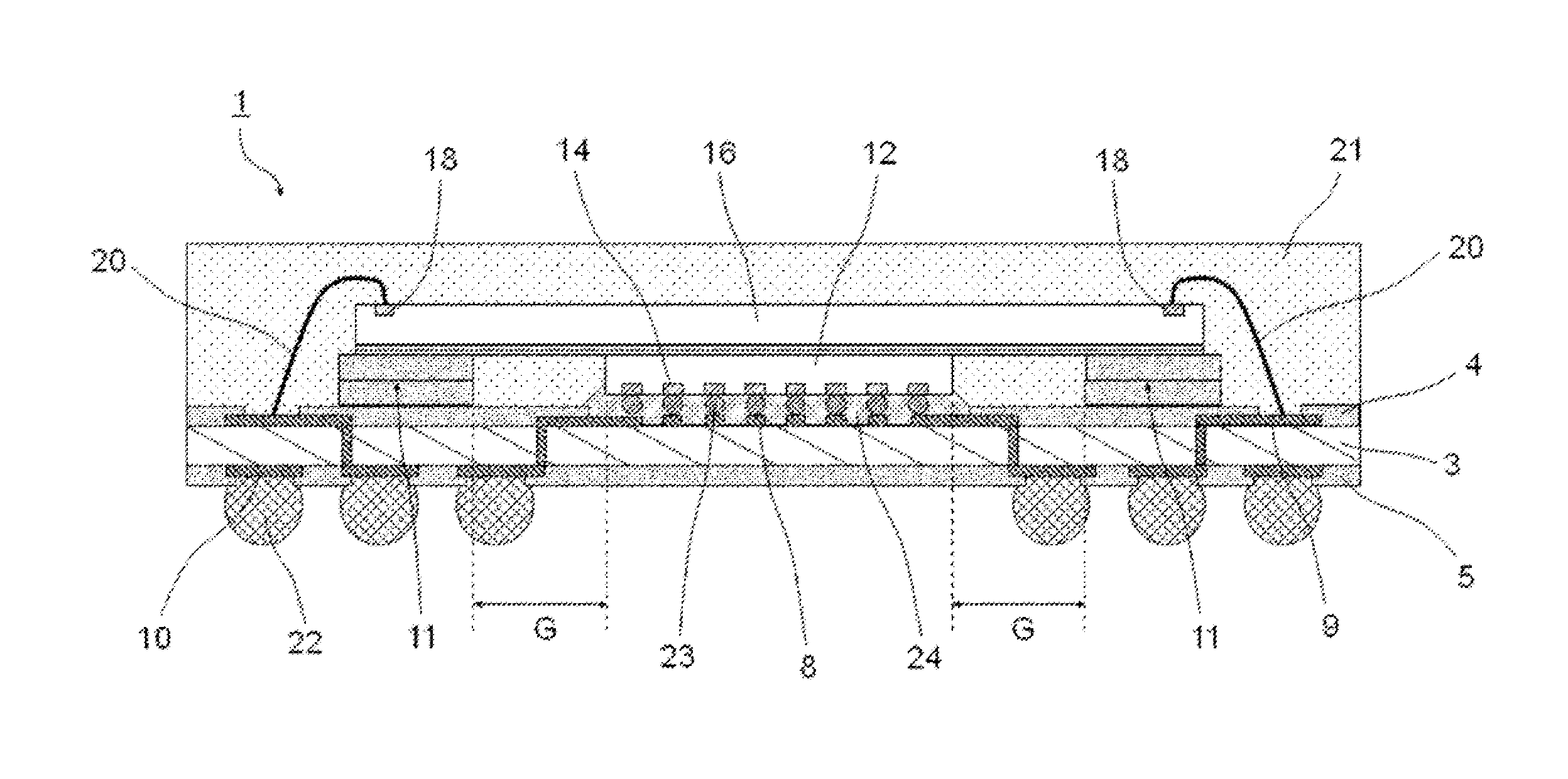
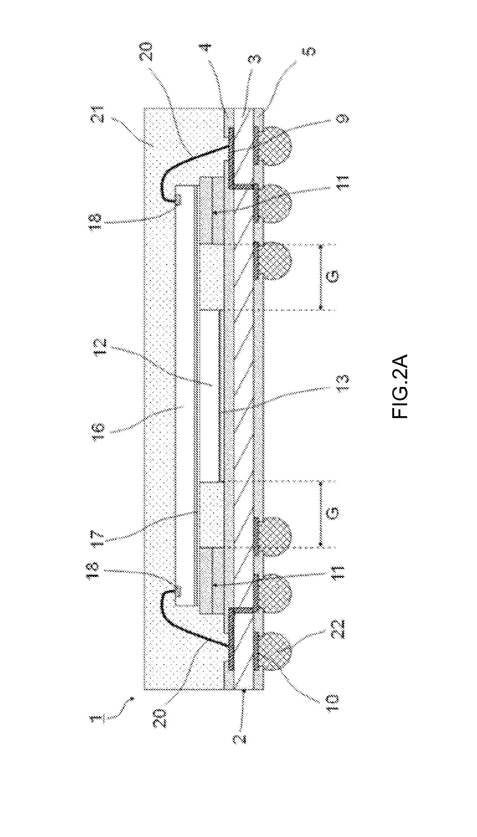
- Description
- Claims
- Application Information
AI Technical Summary
Problems solved by technology
Method used
Image

Examples
Example
Embodiment 2
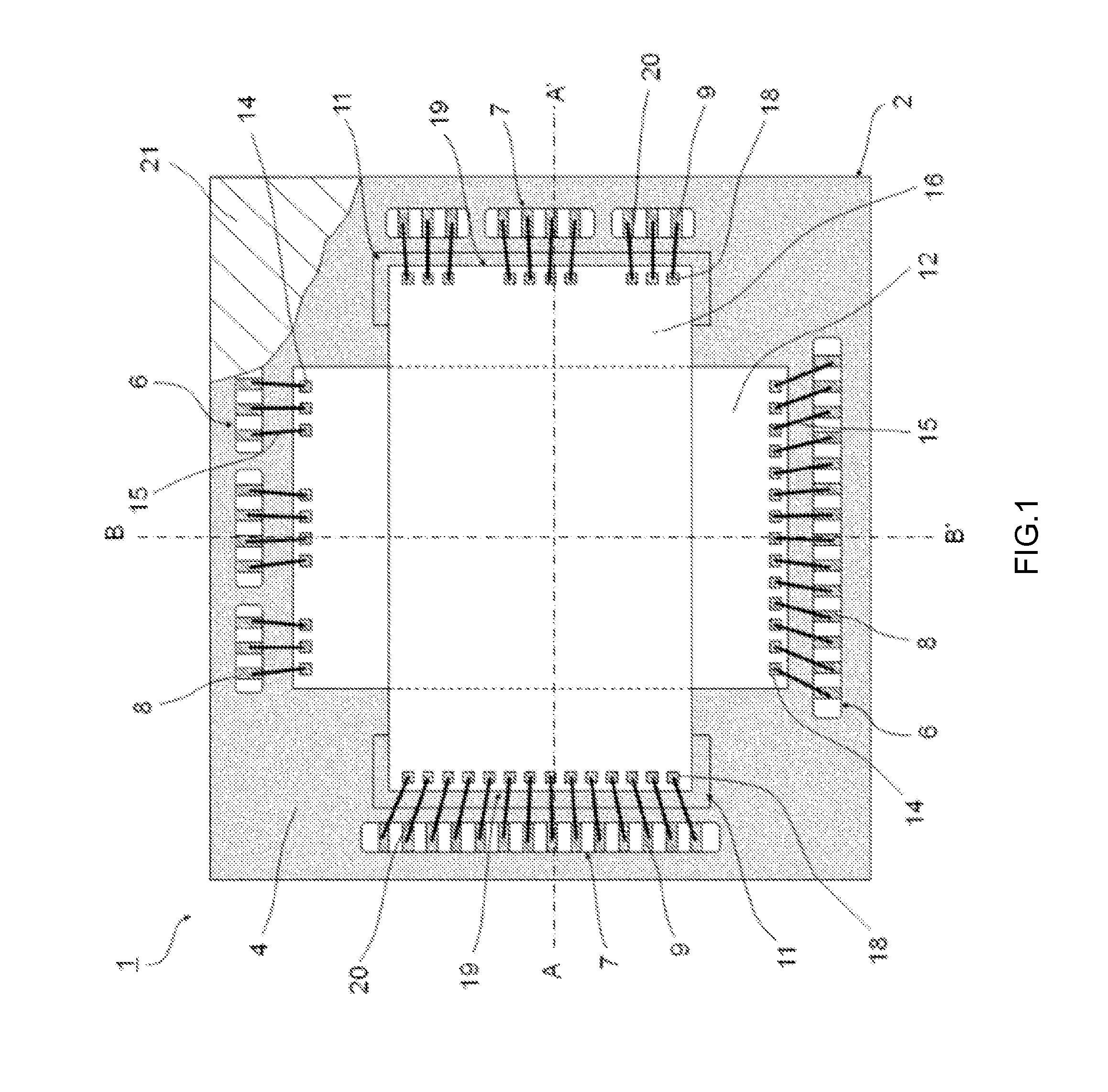
[0057]Referring to FIGS. 8 and 9, the following description will discuss a semiconductor device in accordance with a second embodiment in detail. FIG. 8 is a plan view showing a schematic configuration of a semiconductor device 1 in accordance with the present embodiment. FIG. 9 shows a cross-sectional view that indicates a cross-sectional configuration taken between C-C′ of FIG. 8.
[0058]The semiconductor device 1 relating to the present embodiment is configured in the same manner as in the semiconductor device (see FIGS. 1, 2A and 2B) of the first embodiment. However, as shown in FIGS. 8 and 9, the semiconductor device 1 of the present embodiment is different from the semiconductor device relating to the first embodiment in that the first semiconductor chip 12 is disposed so as to be shifted toward one of the short sides of the second semiconductor chip 16, and in that only one of the short sides 19 of the second semiconductor chip 16 is overhanged, with the overhang po...
Example
Embodiment 3
[0061]Next, referring to FIG. 10, the following description will discuss a semiconductor device in accordance with a third embodiment. FIG. 10 is a cross-sectional view showing a schematic configuration of a semiconductor device 1 in accordance with the present embodiment.
[0062]The semiconductor device 1 relating to the present embodiment is configured in the same manner as in the semiconductor device (see FIGS. 1, 2A and 2B) of the first embodiment. However, as shown in FIG. 10, the semiconductor device 1 of the present embodiment is different from the semiconductor device relating to the first embodiment in that bump electrodes 23 are formed on the electrode pads 14 of the first semiconductor chip 12 so that the first semiconductor chip 12 is flip-chip assembled on the first connection pads 8 of the wiring substrate 2, with the bump electrodes 23 interposed therebetween.
[0063]The thick film portion 11 is desirably adjusted so that the gap G between the thick film porti...
PUM
 Abstract
Description
Claims
Application Information
 - R&D Engineer
- R&D Manager
- IP Professional
- Industry Leading Data Capabilities
- Powerful AI technology
- Patent DNA Extraction
Browse by: Latest US Patents, China's latest patents, Technical Efficacy Thesaurus, Application Domain, Technology Topic.
© 2024 PatSnap. All rights reserved.Legal|Privacy policy|Modern Slavery Act Transparency Statement|Sitemap