

Semiconductor device and production method
a technology of semiconductor devices and production methods, applied in semiconductor devices, electrical devices, transistors, etc., can solve the problems of difficult further downsizing, inconvenient contamination of semiconductor devices produced by that manufacturing equipment, and difficulty in leaking current control, so as to reduce metal contamination of gate etching devices and reduce metal contamination of nitride film wet etching devices
- Summary
- Abstract
- Description
- Claims
- Application Information
AI Technical Summary
Benefits of technology
Problems solved by technology
Method used
Image

Examples
embodiment 1
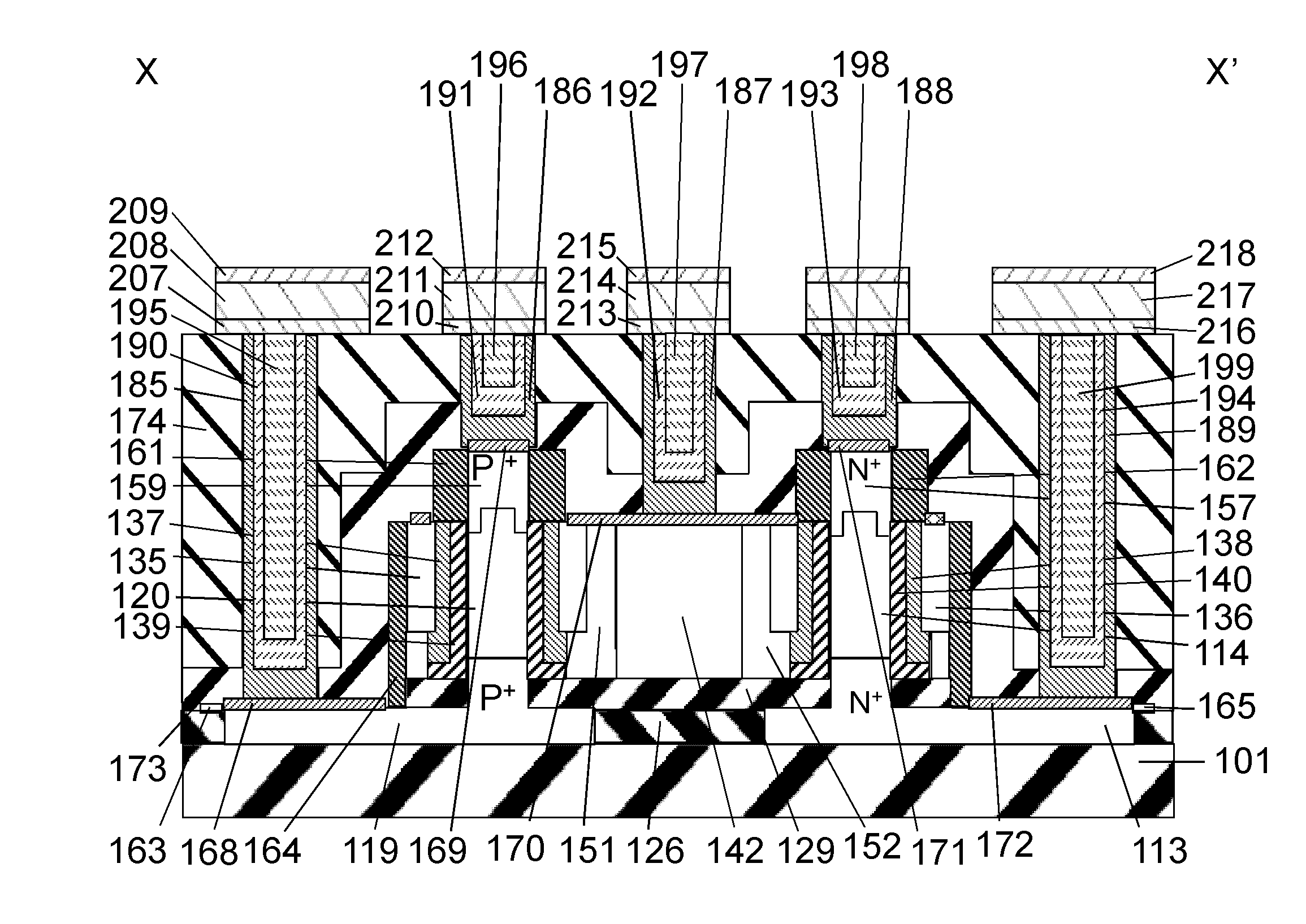
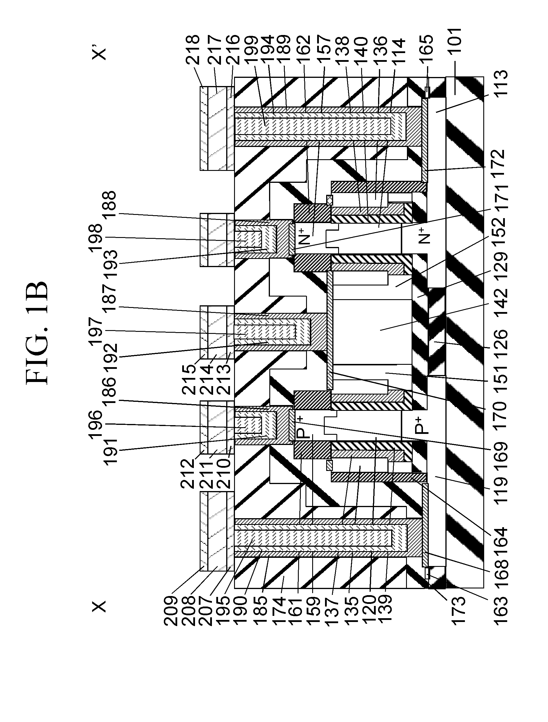
[0636]FIG. 1C shows an SGT 220 according to a first embodiment of the present invention.
[0637]This SGT 220 is an nMOS SGT and is provided with a first planar silicon layer 234 and a first columnar silicon layer 232 formed on top of the first planar silicon layer 234.
[0638]A first n+ type silicon layer 113 is formed on the lower region of the first columnar silicon layer 232 and the region of the first planar silicon layer 234 positioned below the first columnar silicon layer 232, and a second n+ type silicon layer 157 is formed on the upper region of the first columnar silicon layer 232. In this embodiment, the first n+ type silicon layer 113, for example, functions as a source scattering layer and the second n+ type silicon layer 157 functions as a drain scattering layer. In addition, the area between the source scattering layer and the drawing scattering layer functions as a channel region. The first columnar silicon layer 232 between the first n+ type silicon layer 113 and the se...
embodiment 2
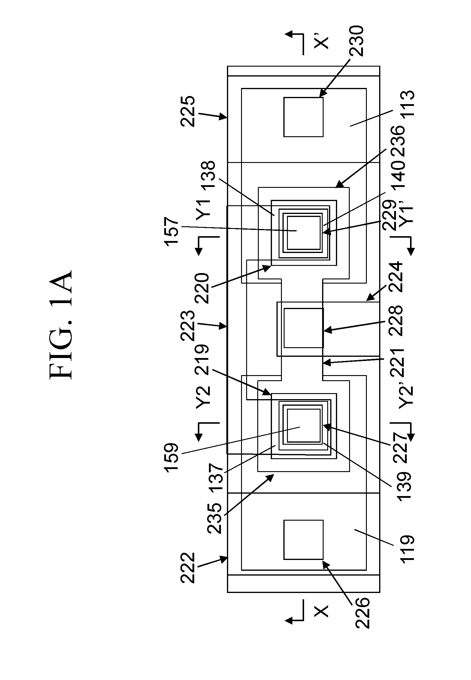
[0651]In the first embodiment, an example was shown of a single columnar semiconductor layer, but in the second embodiment, an example is shown of a circuit composed of multiple columnar semiconductor layers.
[0652]An inverter according to the second embodiment is provided with a pMOS SGT and an nMOS SGT.
[0653]The nMOS SGT 220 is provided with a first planar silicon layer 234 and a first columnar silicon layer 232 formed on top of the first planar silicon layer 234.
[0654]A first n+ type silicon layer 113 is formed on the lower region of the first columnar silicon layer 232 and the region of the first planar silicon layer 234 positioned below the first columnar silicon layer 232, and a second n+ type silicon layer 157 is formed on the upper region of the first columnar silicon layer 232. In this embodiment, the first n+ type silicon layer 113, for example, functions as a source scattering layer and the second n+ type silicon layer 157 functions as a drain scattering layer. In addition...
PUM
 Abstract
Description
Claims
Application Information