Poly silicon hard mask

a technology of polysilicon and hard mask, which is applied in the direction of semiconductor devices, semiconductor/solid-state device details, electrical apparatus, etc., can solve the problems of easy damage to low-k dielectric materials, difficult to meet escalating requirements, and difficult handling of low-k materials such as bcb, etc., to reduce the contamination of etching chamber metals

Inactive Publication Date: 2008-05-29
TAIWAN SEMICON MFG CO LTD
View PDF5 Cites 6 Cited by
  • Summary
  • Abstract
  • Description
  • Claims
  • Application Information

AI Technical Summary

Benefits of technology

[0014]It is still another object of the present disclosure to present a method for reducing etching chamber metal contamination during etching of low-k dielectric layer with a hard mask. In one embodiment, the method includes etching the hard mask with a gas plasma to create exposed portions of the low-k dielectric layer, stripping the photoresist layer and etching the exposed portions of low-k dielectric layer. The hard mask can include a polysilicon layer for eliminating metal contamination in the etching chamber.

Problems solved by technology

Such escalating requirements have been found difficult to satisfy in terms of providing a low RC (resistance capacitance) interconnection pattern, particularly where sub-micron via contacts and trenches have high aspect ratios imposed by miniaturization.
However, low k materials such as benzocyclobutene (BCB), hydrogen silsesquioxane (HSQ), SiOF, etc., are often more difficult to handle than traditionally employed higher k materials, such as an oxide.
For example, low k dielectric materials are readily damaged by techniques used to remove photoresist materials after the patterning of a layer.
Hence, a feature formed in a low k dielectric layer may be damaged when the photoresist mask used to form the feature (e.g., trench or via) is removed.
Other problems that have been observed when working with low k materials are those of via poisoning and resist scumming.
This out gassing problem leads to improperly formed topology on the wafer.
The resist around the via hole 20 becomes very thick and difficult to pattern.
When attempts are made to pattern and expose it, that area can not be exposed properly.
Two technical challenges in advanced technology node of 65 nm and beyond are related to the problems associated with low-k dielectrics.
Insufficient thickness of photoresist for the better profile control is a dilemma between lithographs and etch.
Although this has been seen to help the via poisoning problem, it does not substantially eliminate the problem.
Other methodology that has been attempted is to provide spin-on organic BARC in the via, but the relatively low adhesion of this material to the via sidewalls and bottom has caused this approach to fail in substantially eliminating via poisoning concerns.
Another method to eliminate via poisoning concerns is to provide a thick layer of oxide within the via, but this has the disadvantage of undesirably reducing the via size.
Other attempts have included depositions of relatively thick layers of organic and inorganic BARCs within and on top of the via, but such attempts have the undesired effect of requiring a photoresist layer substantially as thick as the BARC layer.
Such a thickness is undesirably large, resulting in less accurate patterning than that achievable with a relatively thinner photoresist layer.
The introduction of any additional layers underneath the photoresist masks to allow for reduction of the photoresist layer thickness should not, however, have the undesirable side effects of increasing processing time and costs or increasing the likelihood of damage to underlying layers of materials.
However, low-k damage is still an issue which has not been solved in the prior art.
However, oxide chamber suffers short lifetime because of metal contamination and thus is a fatal issue in terms of production costs.
The photoresist including the tri-layer approach still allows damage in the low-k dielectric and increased photoresist use and cost and requires three layers (photoresist, cap and organic layer) which are costly.
The other approach described above is the use of a metal hard mask, which unfortunately as noted above causes contamination of the etch / ash chamber and thus reduces the lifetime of the chamber and creates the extra burden for metal residue removal.

Method used


Image

  • Poly silicon hard mask
  • Poly silicon hard mask
  • Poly silicon hard mask

Examples


Embodiment Construction

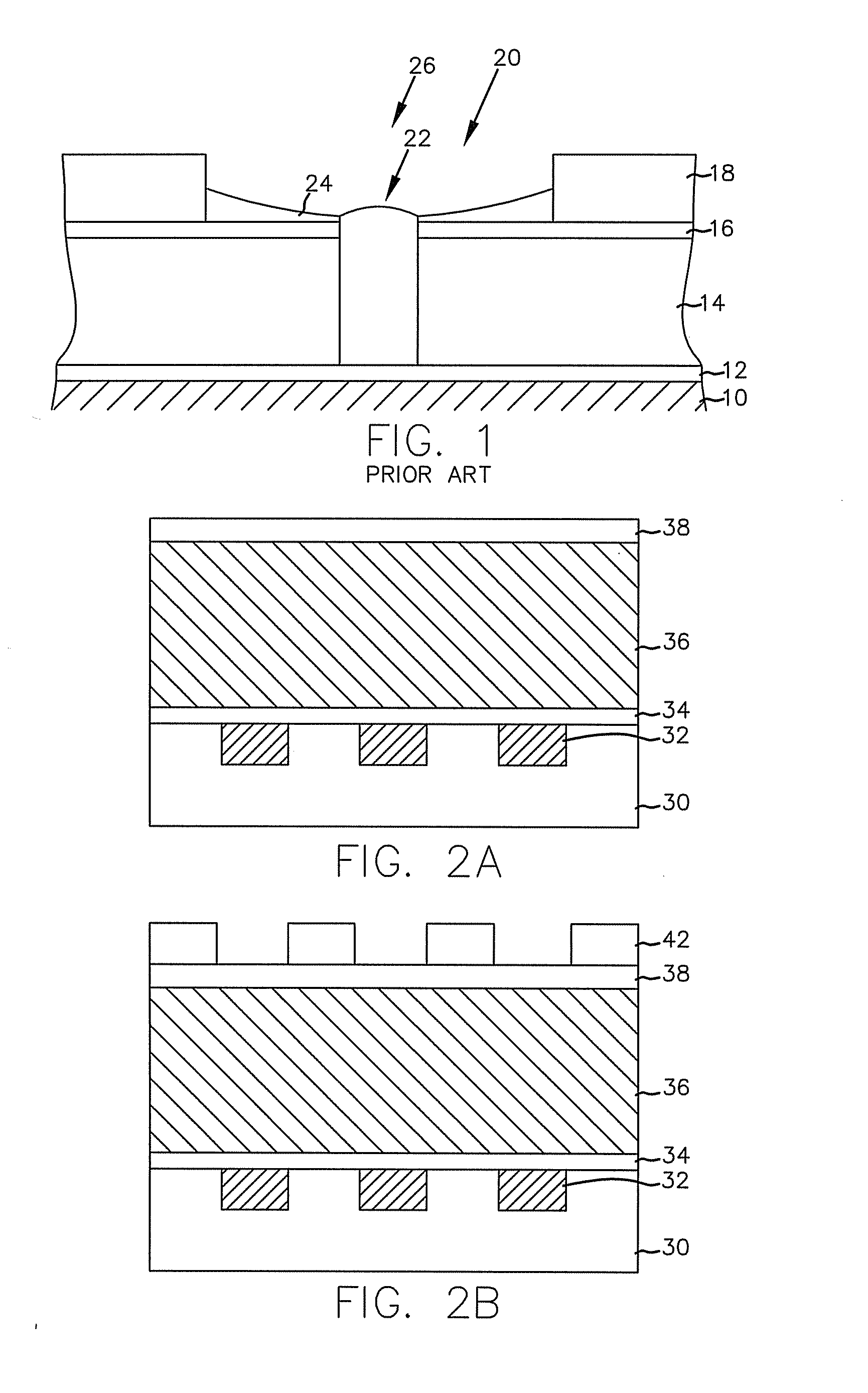
[0019]In one embodiment, the disclosure relates to using polysilicon as hard mask in place of, or instead of, the metal hard mask layer. Polysilicon has an etch rate much less than the etch rate of the dielectric layer thereby providing excellent selectivity as the hard mask layer. There is no metal contamination problem with polysilicon which plagues the prior art production methods. The ability and knowledge of patterning polysilicon is well developed. Polysilicon minimizes low-k damage by blocking energetic ions from impinging onto and penetrating into the low-k film perpendicularly and shifts the resist strip step from the end of the patterning sequence to before the dielectric etch step.

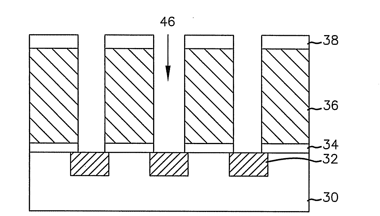
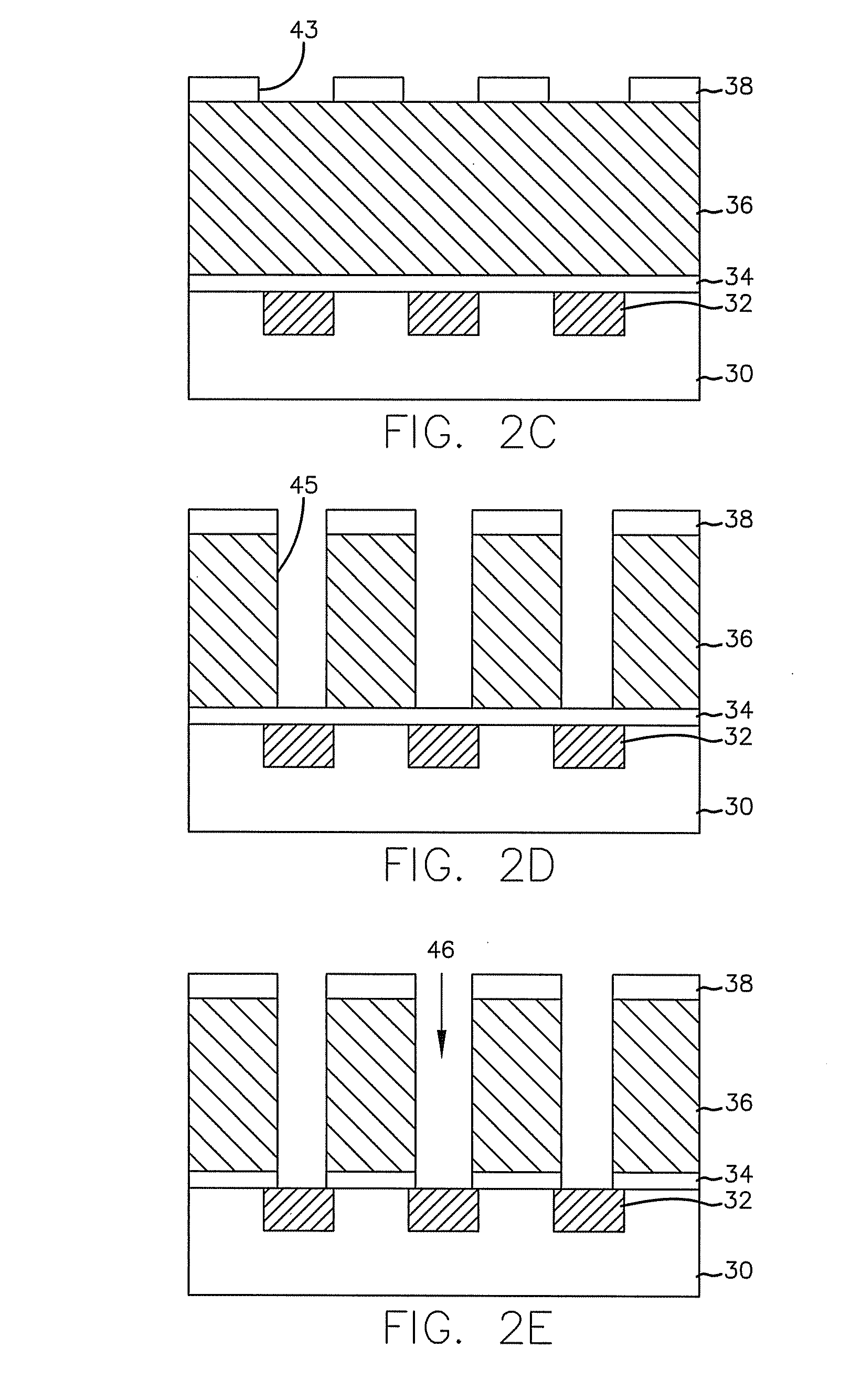
[0020]FIGS. 2A to 2E are cross-sectional diagrams showing an exemplary process according to an embodiment of the disclosure. As shown in FIG. 2A, a semiconductor substrate 30 comprises a plurality of metal wire structures 32, a dielectric separation layer 34 covering the metal wire structures 32...


PUM

PropertyMeasurementUnit
temperatureaaaaaaaaaa
dielectric constantaaaaaaaaaa

Abstract

A method of forming an opening on a low-k dielectric layer using a polysilicon hard mask rather than a metal hard mask as used in prior art. A polysilicon hard mask is formed over a low-k dielectric layer and a photoresist layer is formed over the polysilicon hard mask. The photoresist layer is patterned and the polysilicon hard mask is etched with a gas plasma to create exposed portions of the low-k dielectric layer. The photoresist layer in stripped prior to the etching of the exposed portions of the low-k dielectric layer to avoid damage to the low-k dielectric layer.

Description

BACKGROUND[0001]The escalating requirements for high-density and performance associated with ultra large-scale integration semiconductor wiring require responsive changes in interconnection technology. Such escalating requirements have been found difficult to satisfy in terms of providing a low RC (resistance capacitance) interconnection pattern, particularly where sub-micron via contacts and trenches have high aspect ratios imposed by miniaturization.[0002]Conventional semiconductor devices typically comprise a semiconductor substrate, normally of doped monocrystalline silicon, and a plurality of sequentially formed dielectric layers and conductive patterns. An integrated circuit is formed containing a plurality of conductive patterns comprising conductive lines separated by inter-wiring spacing. Typically, the conductive patterns on different layers, i.e., upper and lower layers, are electrically connected by a conductive plug filling a via hole, while a conductive plug filling a ...

Claims


Application Information

Patent Timeline
Patent Type & Authority Applications(United States)
IPC IPC(8): H01L23/52H01L21/311
CPCH01L21/31144H01L21/76811H01L21/76802
Inventor TSAI, JANG-SHIANGSHIEH, JYU-HORNGHSU, JU-WANGCHEN, DE-FANGLIN, CHIA-HUIJANG, SYUN-MING
Owner TAIWAN SEMICON MFG CO LTD
Why Eureka
Try Eureka