Method for manufacturing semiconductor integrated circuit device

a technology of integrated circuit and semiconductor, which is applied in the direction of semiconductor devices, electrical equipment, transistors, etc., can solve the problems of severe restriction of leak current value, difficult to adopt polymetal gate for the product, and high leak curren

Inactive Publication Date: 2007-08-16
SEMICON PATENT
View PDF6 Cites 5 Cited by
  • Summary
  • Abstract
  • Description
  • Claims
  • Application Information

AI Technical Summary

Benefits of technology

[0011] An object of the present invention is to reduce the leak current of the MISFET by reducing the contamination of the metal composing the polymetal gate.
[0012] Also, another object of the present invention is to improve the retention characteristic of a memory cell including the MISFET by reducing the leak current in the MISFET.
[0013] Also, another object of the present invention is to improve the performance of the semiconductor integrated circuit device having the MISFET by reducing the leak current in the MISFET. Still another object of the present invention is to improve the yield of the semiconductor integrated circuit device.

Problems solved by technology

However, it had been frequently found that the product adopting such a polymetal gate structure has a tendency to increase the leak current.
As a result, it had been difficult to adopt the polymetal gate for the product with severe restriction in the leak current value.

Method used


Image

  • Method for manufacturing semiconductor integrated circuit device
  • Method for manufacturing semiconductor integrated circuit device
  • Method for manufacturing semiconductor integrated circuit device

Examples


Embodiment Construction

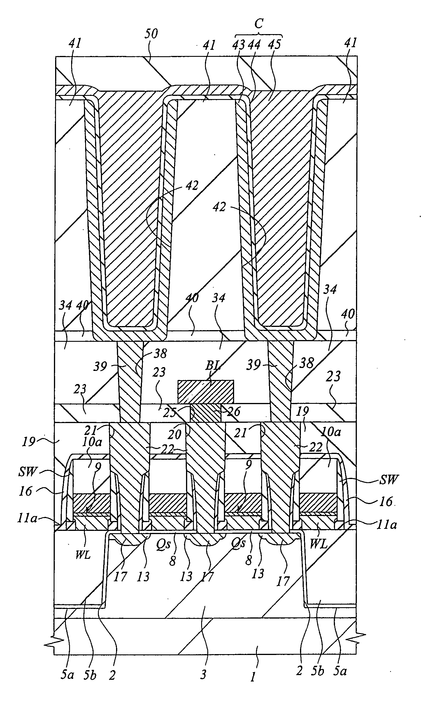
[0050] Hereinafter, an embodiment of the present invention will be described in detail based on the accompanying drawings. Note that, in all of the drawings for describing the embodiments, components having the same function are denoted by the same reference symbols and the repetitive descriptions thereof will be omitted.

[0051] The method of manufacturing a DRAM according to the embodiment of the present invention will be described with reference to FIGS. 1 to 18 along with the manufacturing steps performed.

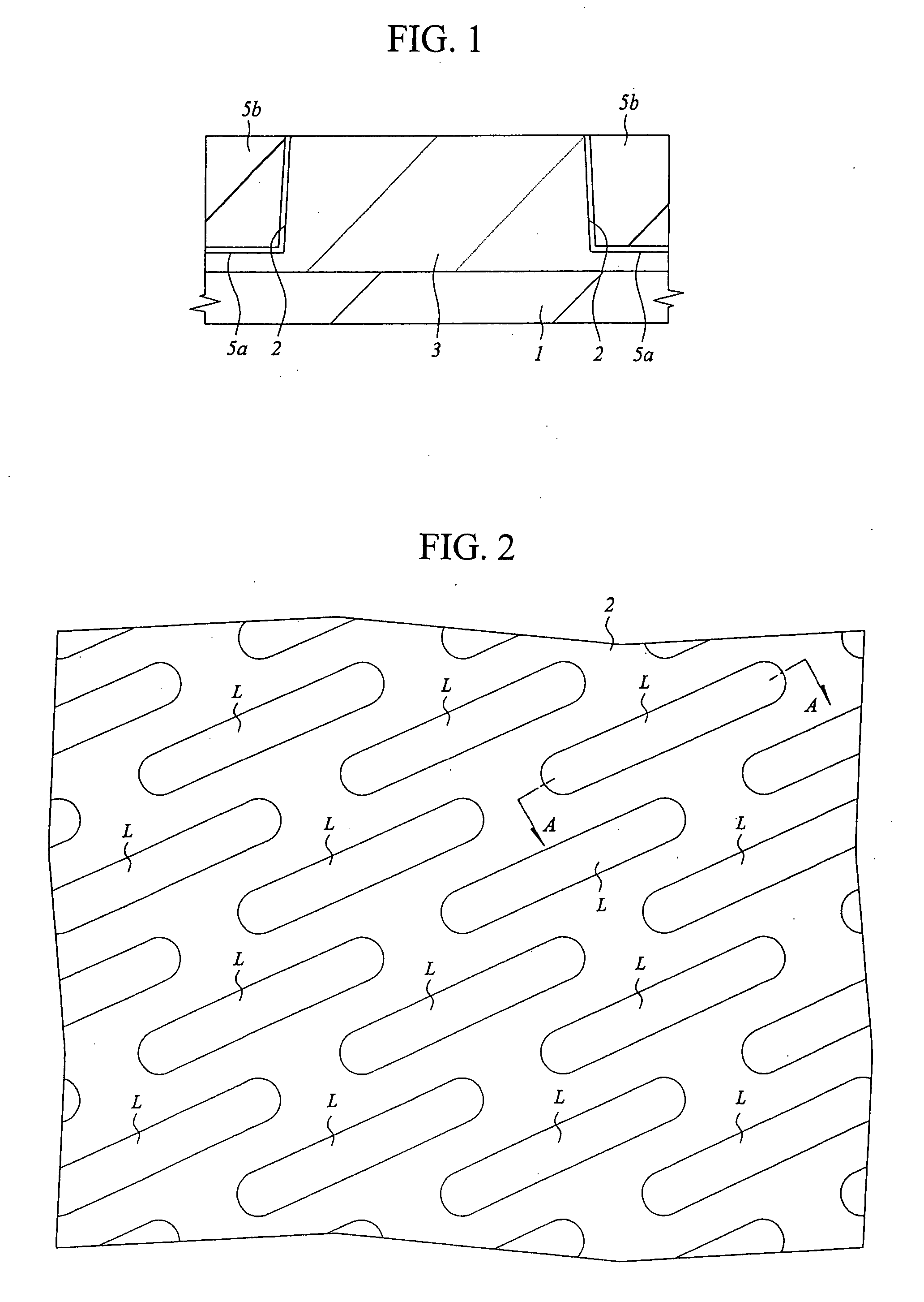
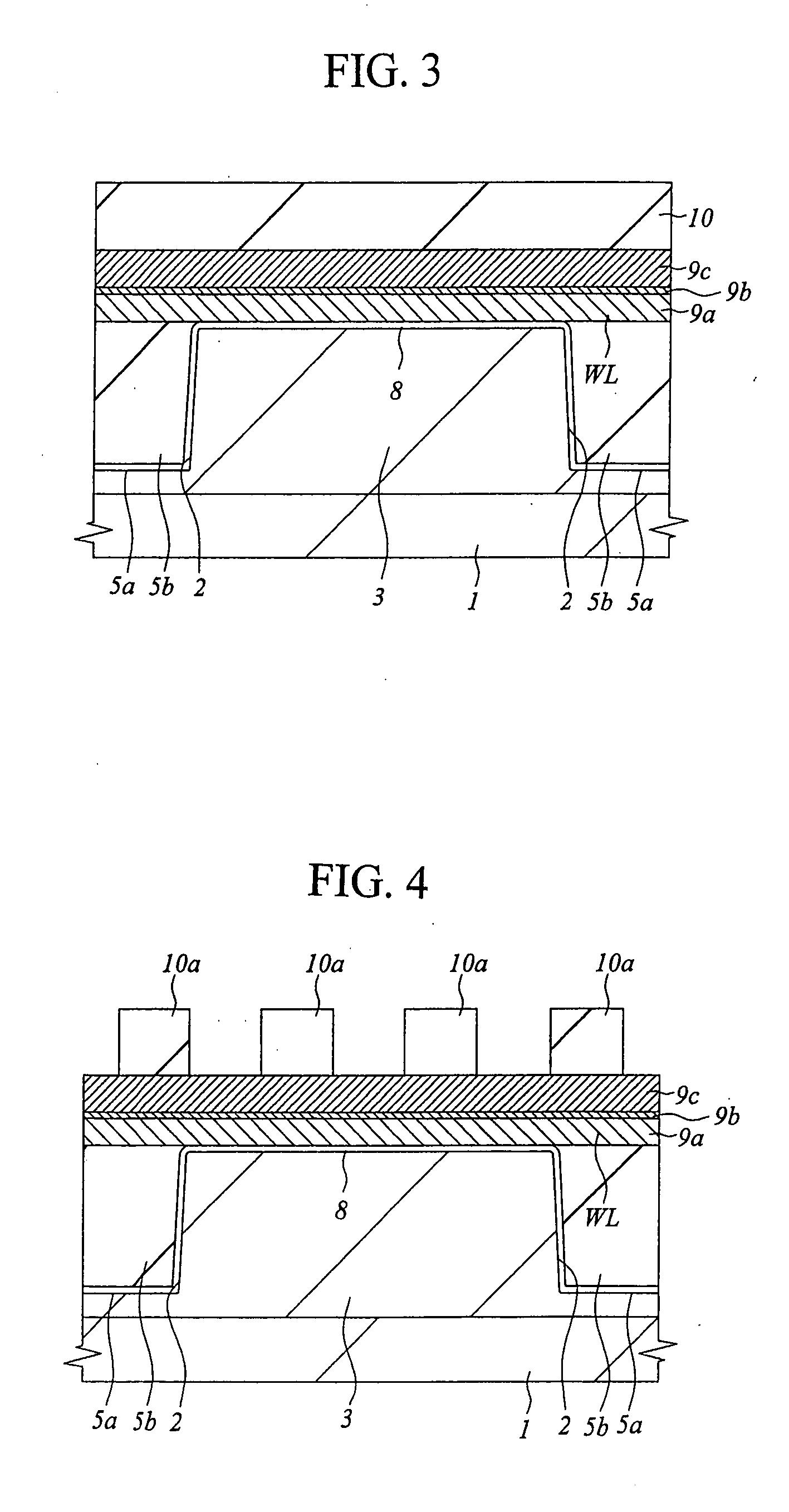
[0052] First, as shown in FIG. 1, a semiconductor substrate 1 made of p-type single crystal silicon having the specific resistance of about 1 to 10 Ωcm is etched to form an element isolation trench with a depth of about 350 nm.

[0053] Then, the thermal oxidation at about 1000° C. is performed to the semiconductor substrate 1, thereby forming a thin silicon oxide film 5a with a thickness of about 10 nm on an inner wall of the trench. The silicon oxide film 5a is formed in order ...


PUM


Abstract

Disclosed is a technique for reducing the leak current by reducing contamination of metal composing a polymetal gate of a MISFET. Of a polycrystalline silicon film, a WN film, a W film, and a cap insulating film formed on a gate insulating film on a p-type well (semiconductor substrate), the cap insulating film, the W film, and the WN film are etched and the over-etching of the polycrystalline silicon film below them is performed. Then, a sidewall film is formed on sidewalls of these films. Thereafter, after etching the polycrystalline silicon film with using the sidewall film as a mask, a thermal treatment is performed in an oxidation atmosphere, by which a light oxide film is formed on the sidewall of the polycrystalline silicon film. As a result, the contamination on the gate insulating film due to the W and the W oxide can be reduced, and also, the diffusion of these materials into the semiconductor substrate (p-type well) and the resultant increase of the leak current can be prevented.

Description

CROSS REFERENCE TO RELATED APPLICATION [0001] This application is a continuation application of U.S. Ser. No. 10 / 978,469, filed Nov. 2, 2004 which is a continuation application of U.S. Ser. No. 10 / 223,317, filed Aug. 20, 2002, the contents of which are incorporated herein by reference.TECHNICAL FIELD OF THE INVENTION [0002] The present invention relates to a semiconductor integrated circuit device and a technique of manufacturing the same, more particularly, the present invention relates to a gate structure of a fine MISFET (Metal Insulator Semiconductor Field Effect Transistor) and a technique effectively applied to a method of manufacturing the same. BACKGROUND OF THE INVENTION [0003] A so-called polymetal gate in which refractory metal such as tungsten is laminated on a polycrystalline silicon film is adopted in order to lower the resistance of the gate electrode of the MISFET. [0004] Meanwhile, a so-called light oxidation treatment for forming a thermal oxide film on a sidewall ...

Claims


Application Information

Patent Timeline
Patent Type & Authority Applications(United States)
IPC IPC(8): H01L29/94H01L21/28H01L21/768H01L21/60H01L21/8242H01L27/092H01L27/108H01L29/49H01L29/78
CPCH01L21/28061H01L21/28247H01L21/76897H01L29/4983H01L27/10814H01L27/10873H01L29/4941H01L27/10811H10B12/312H10B12/315H10B12/05H01L27/092
Inventor KUJIRAI, HIROSHIOKUYAMA, KOUSUKEHATA, KAZUHIROOYU, KIYONORINAGAI, RYOUCHIYAMA, HIROYUKIKUMAUCHI, TAKAHIROICHISE, TERUHISA
Owner SEMICON PATENT
Why Eureka
Try Eureka