Semiconductor device

a technology of semiconductors and semiconductors, applied in the field of semiconductor devices, can solve the problems of difficult to reduce power consumption satisfactorily, short data holding period, loss of memory content, etc., and achieve the effect of easy multi-value information

Active Publication Date: 2011-05-26
SEMICON ENERGY LAB CO LTD
View PDF99 Cites 127 Cited by
  • Summary
  • Abstract
  • Description
  • Claims
  • Application Information

AI Technical Summary

Benefits of technology

[0010]In view of the above problem, one object of one embodiment of the present invention is to provide a semiconductor device having a new structure, the semiconductor device being capable of holding memory content in the state where power is not supplied and having no limitation on the number of writing operations. Another object of one embodiment of the present invention is to provide a semiconductor having a structure allowing using easily multivalued information.
[0030]A transistor using an oxide semiconductor has extremely low off-state current; therefore, by using the transistor, memory content can be stored for a relatively long time. That is, refresh operation can become unnecessary, or frequency of refresh operation can be reduced considerably, so that power consumption can be reduced substantially. Further, even in the case where power is not supplied, memory content can be stored for a long time.
[0031]In addition, high voltage is not needed for writing information in the semiconductor device and there is no problem of deterioration of elements. For example, since there is no need to perform injection of electrons to a floating gate and extraction of electrons from a floating gate which are needed in a conventional nonvolatile memory, deterioration such as deterioration of a gate insulating layer does not occur. That is, the semiconductor device according to one embodiment of the present invention does not have a limit on the number of times of writing which is a problem in a conventional nonvolatile memory, and reliability thereof is drastically improved. Further, information is written according to an on state and an off state of the transistor, whereby high-speed operation can be easily realized. Additionally, when information is written, there is an advantage that operation for erasing the previously stored information is not needed.
[0032]Further, the transistor formed using a material other than an oxide semiconductor can be operated at sufficiently high speed; therefore, by using the transistor, stored contents can be read out at high speed.
[0033]Moreover, the semiconductor device according to one embodiment of the present invention can easily multivalue data by being provided with a boosting circuit, so that storage capacity can be increased.

Problems solved by technology

In addition, there is leakage of current in a transistor included in a memory element so that a charge accumulated at an electrode of the capacitor is lost or a charge flows into the capacitor, even if the transistor is not selected to perform any operation, whereby data holding period is short.
Therefore, it is necessary to perform rewriting in a predetermined cycle (refresh operation) and it is difficult to reduce power consumption satisfactorily.
Further, since memory content is lost when the power is not supplied to the DRAM, another memory device using a magnetic material or an optical material is needed to store information for a long period.
However, an inconvenient in that a cost per storage capacity becomes high because a circuit such as a flip flop is used.
Further, in view of the point that memory content is lost when the power is not supplied, an SRAM is not superior to a DRAM.
However, in flash memory, there is a problem in that a memory element does not function after performing writing operations a predetermined number of times because a gate insulating layer included in the memory element is deteriorated by a tunnel current occurring each time a writing operation is performed.
However, a complicated peripheral circuit is needed to apply this method.
Further, even if such a method is employed, the basic problem of lifetime is not resolved.
That is, a flash memory is unsuitable for applications in which information is rewritten with high frequency.
Further, high voltage is required to store a charge in the floating gate or to remove a charge in the floating gate.
Furthermore, a relatively long time is required for storing or removing a charge and the speed of writing and erasing cannot easily be increased.

Method used


Image

  • Semiconductor device
  • Semiconductor device
  • Semiconductor device

Examples


embodiment 1

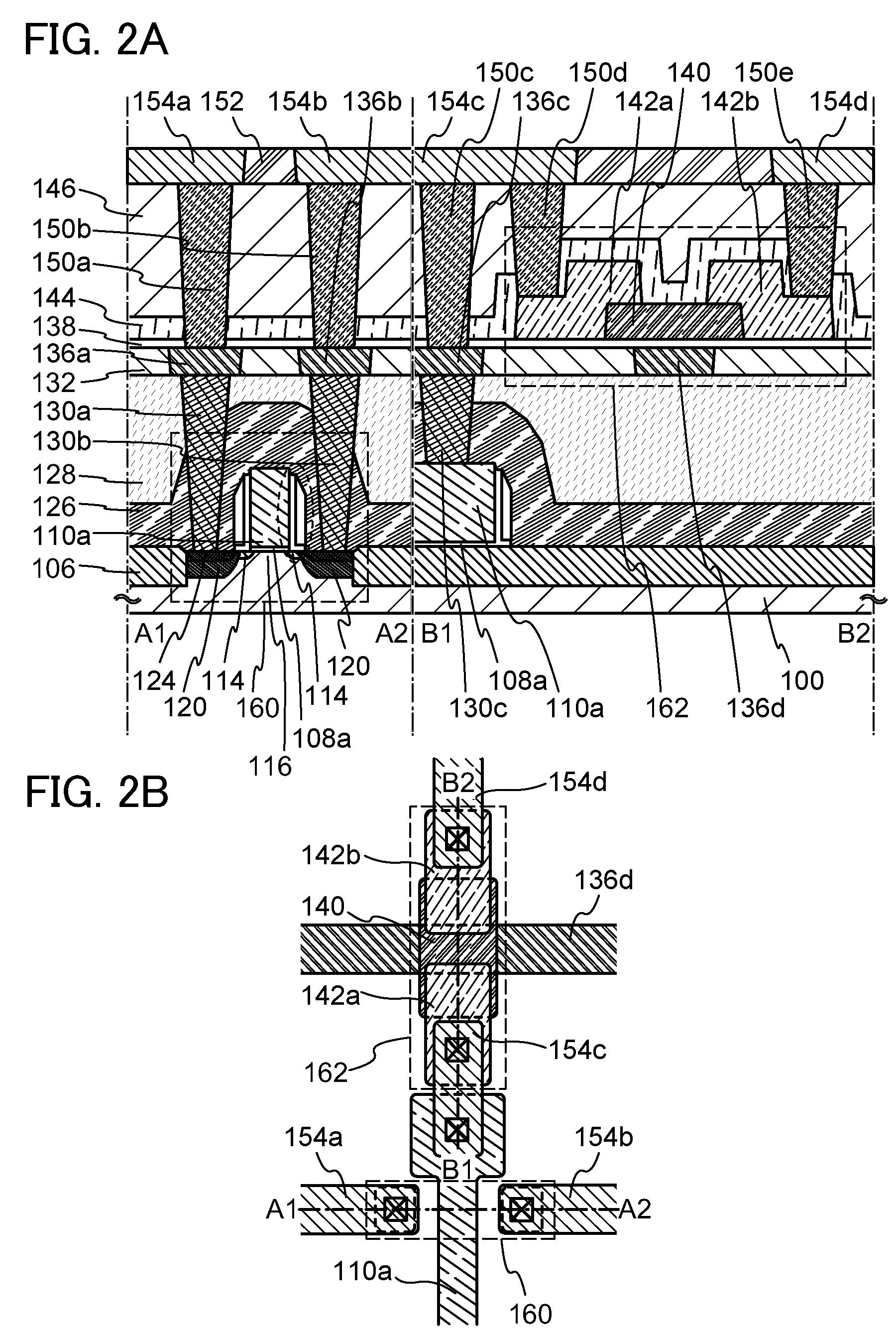
[0077]In this embodiment, structures and manufacturing methods of semiconductor devices according to one embodiment of the disclosed invention are described with reference to FIG. 1, FIGS. 2A and 2B, FIGS. 3A to 3H, FIGS. 4A to 4G, FIGS. 5A to 5D, FIG. 6, FIGS. 7A and 7B, FIGS. 8A and 8B, FIG. 9, FIG. 10, FIG. 11, FIG. 12, FIGS. 13A and 13B, FIGS. 14A and 14B, and FIGS. 15A and 15B.

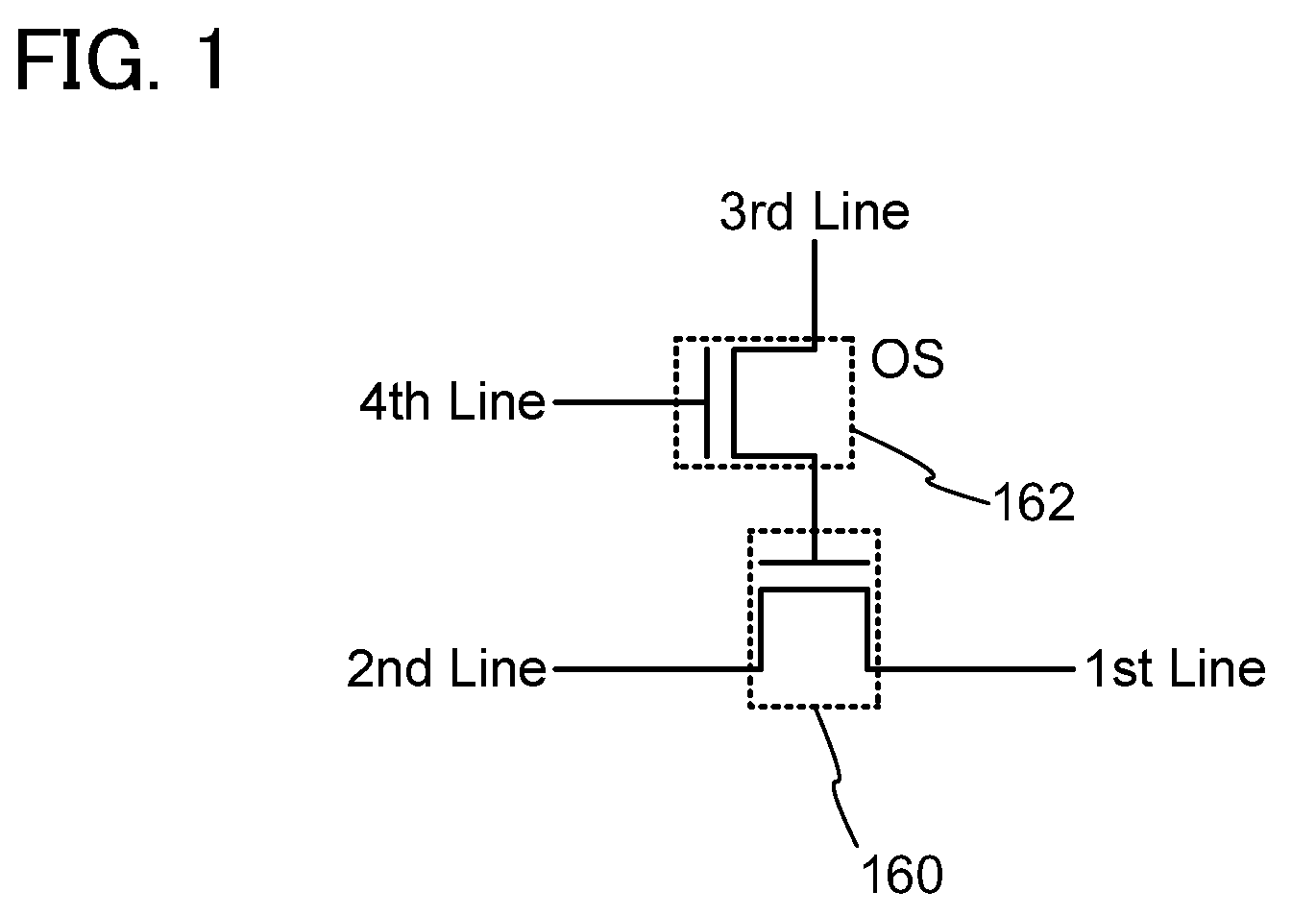
[0078]FIG. 1 illustrates an example of a circuit configuration of a semiconductor device. The semiconductor device includes a transistor 160 which uses a material other than an oxide semiconductor and a transistor 162 which uses an oxide semiconductor. Note that a mark “OS” is added to the transistor 162 in FIG. 1 to show that the transistor 162 uses an oxide semiconductor.

[0079]Here, a gate electrode of the transistor 160 is electrically connected to one of a source electrode and a drain electrode of the transistor 162. A first wiring (which is denoted as “1st Line” and also called a source line) and a s...

embodiment 2

[0234]In this embodiment, a circuit configuration and operation of a semiconductor device according to one embodiment of the present invention will be described.

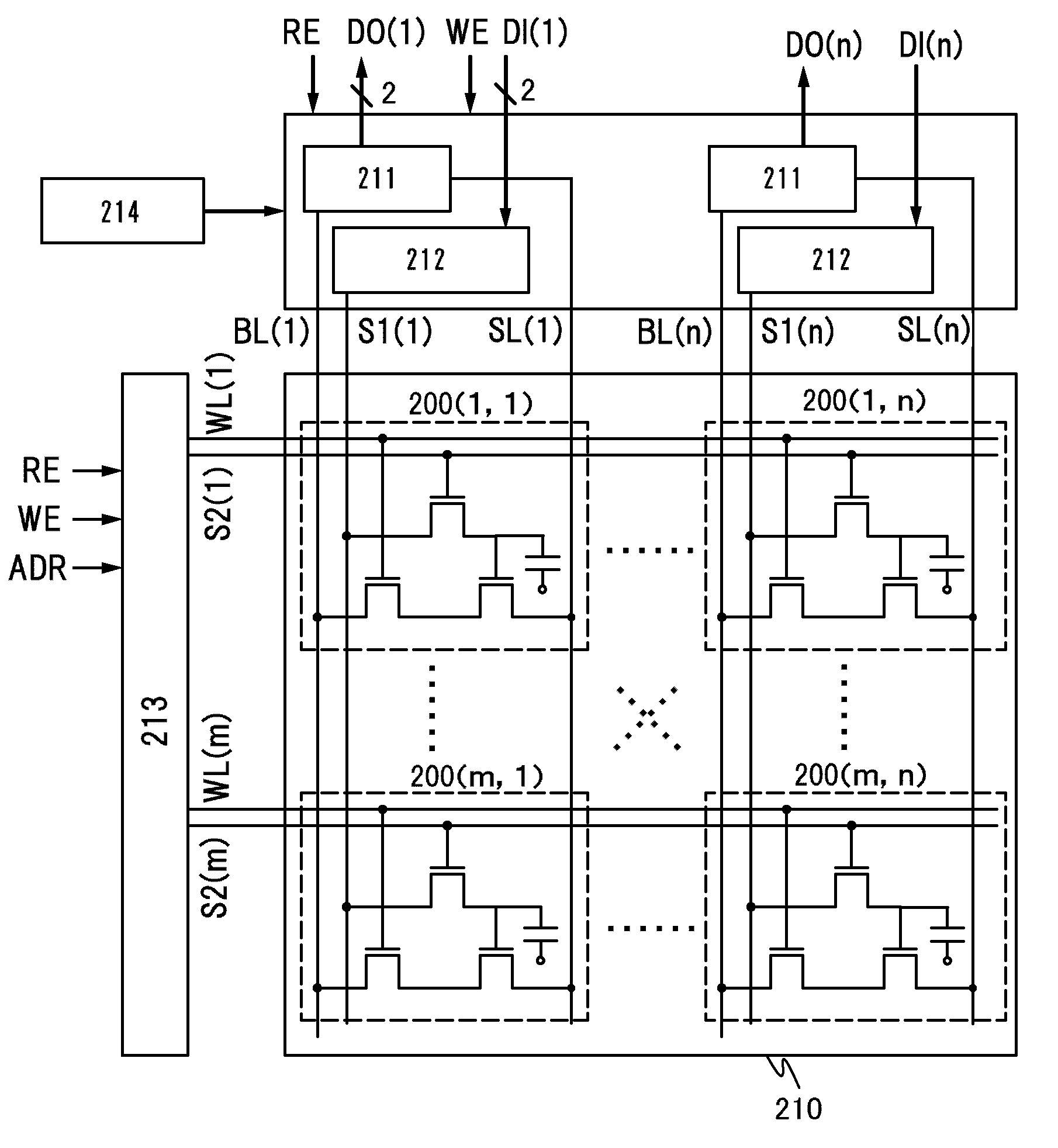
[0235]An example of a circuit diagram of a memory element (hereinafter also referred to as a memory cell) including the semiconductor device is illustrated in FIG. 16. A memory cell 200 illustrated in FIG. 16 is a multi-valued memory cell and includes a source line SL, a bit line BL, a first signal line S1, a second signal line S2, a word line WL, a transistor 201, a transistor 202, a transistor 203, and a capacitor 205. The transistors 201 and 203 are formed using a material other than an oxide semiconductor, and the transistor 202 is formed using an oxide semiconductor.

[0236]Here, a gate electrode of the transistor 201 is electrically connected to one of a source electrode and a drain electrode of the transistor 202. In addition, the source line SL is electrically connected to a source electrode of the transistor 201, and ...

embodiment 3

[0283]In this embodiment, a circuit configuration and operation of a semiconductor device according to one embodiment of the present invention are described.

[0284]In this embodiment, a reading operation different from that of Embodiment 2 is described with the use of a circuit configuration of a memory element illustrated in FIG. 16. Note that the capacitor 205 shown in FIG. 16 is not always necessary and can be omitted in some cases. The memory element considered is a multivalued memory element, and a case where the memory element is a four-valued memory element is described in this embodiment. Four states of a memory cell 200 are data “00b”, “01b”, “10b”, and “11b”, and corresponding potentials of a node A are V00, V01, V10, and V11 (V00011011), respectively.

[0285]When writing is performed to the memory cell 200, the source line SL is set to 0 [V], the word line WL is set to 0 [V], the bit line BL is set to 0 [V], and the second signal line S2 is set to 2 [V]. When the data “00b” ...


PUM


Abstract

An object of the present invention is to provide a semiconductor device combining transistors integrating on a same substrate transistors including an oxide semiconductor in their channel formation region and transistors including non-oxide semiconductor in their channel formation region. An application of the present invention is to realize substantially non-volatile semiconductor memories which do not require specific erasing operation and do not suffer from damages due to repeated writing operation. Furthermore, the semiconductor device is well adapted to store multivalued data. Manufacturing methods, application circuits and driving / reading methods are explained in details in the description.

Description

TECHNICAL FIELD[0001]The present invention relates to a semiconductor device using semiconductor elements and a manufacturing method thereof.BACKGROUND ART[0002]Memory devices using semiconductor elements are roughly classified into volatile memory devices that lose their memory content when power supply is stopped and nonvolatile memory devices that can hold their memory content even when power supply is stopped.[0003]As a typical example of a volatile memory device, a dynamic random access memory (DRAM) is given. In a DRAM, a transistor included in a memory element is selected and an electric charge is accumulated in a capacitor, so that information is memorized.[0004]Owing to the above-described principle, a charge in a capacitor is lost when information data is read in a DRAM; thus, it is necessary to perform rewriting of the information data, so that information is memorized again after the information data reading. In addition, there is leakage of current in a transistor inclu...

Claims


Application Information

Patent Timeline
Patent Type & Authority Applications(United States)
IPC IPC(8): G11C5/06
CPCG11C16/0433G11C7/12H01L21/02554H01L21/02565H01L21/02631H01L27/0688H01L27/105H01L27/108H01L27/115H01L27/11551H01L27/1156H01L27/1225H01L29/7869G11C11/24H01L29/26H01L29/22G11C7/18G11C11/4097G11C5/06G11C5/147G11C16/28H01L2924/0002H10B12/00H10B41/20H10B41/70H10B69/00H01L2924/00H01L23/528H01L27/1207H01L29/24H01L29/78H01L29/78603G11C7/10G11C7/22G11C8/08
Inventor YAMAZAKI, SHUNPEIKOYAMA, JUNKATO, KIYOSHI
Owner SEMICON ENERGY LAB CO LTD
Why Eureka
Try Eureka