Semiconductor memory device

a memory device and semiconductor technology, applied in the direction of transistors, solid-state devices, instruments, etc., can solve the problems of short data retention time, increased power consumption, and loss of charge, so as to reduce the off-state current of the transistor, reduce oxygen vacancy, and reduce impurities

Inactive Publication Date: 2012-10-18
SEMICON ENERGY LAB CO LTD
View PDF1 Cites 10 Cited by
  • Summary
  • Abstract
  • Description
  • Claims
  • Application Information

AI Technical Summary

Benefits of technology

[0028]For the oxide semiconductor film, a material having a bandgap of 2.5 eV or more, preferably 3.0 eV or more may be selected. With use of a material with a bandgap in the above range, the off-state current of the transistor can be reduced. Note that in one embodiment of the present invention, in place of the oxide semiconductor, a material having semiconductor characteristics and a bandgap within the above range may be applied.
[0029]It is preferable that the oxide semiconductor film is highly purified so as to contain as little impurities (such as hydrogen, an alkali metal, an alkaline earth metal, a rare gas, nitrogen, phosphorus, or boron) generating carriers directly or indirectly as possible. Furthermore, it is preferable to reduce oxygen vacancy as much as possible. By reducing impurities and oxygen vacancy in the oxide semiconductor film, generation of carriers in the oxide semiconductor film is suppressed, and the off-state current of the transistor can be reduced.
[0030]As described above, when the off-state current of the third transistor is reduced, the charge accumulated in the capacitor can be retained for a long time, and a non-volatile semiconductor memory device can be obtained.
[0031]When the off-state current of the transistor which controls the potential of the capacitor is reduced, the charge accumulated in the capacitor can be retained for a long time, and a non-volatile semiconductor memory device can be provided.
[0032]In addition, the capacitor is provided along the side surface of the one of the pair of electrodes of the third transistor, whereby the capacitance of the capacitor can be increased without increase in the area occupied by the capacitor. As a result, a highly integrated semiconductor memory device can be provided.
[0033]In addition, the netlike conductive film can prevent the electrostatic breakdown of every memory cell, whereby a highly reliable semiconductor memory device can be provided with a high yield.

Problems solved by technology

In addition, when a transistor included in the DRAM is off, charge is lost due to leakage current (off-state current) between a source and a drain and the like; therefore, a data retention time is short.
Accordingly, a writing operation (a refresh operation) is needed in a predetermined cycle, which results in increase in power consumption.
In addition, data is lost when supply of power is stopped, and thus another memory device using, for example, a magnetic material or an optical material is needed in order to retain data for a long time.
However, there is a problem in that cost per storage capacity becomes high because a circuit such as a flip flop is used.
Moreover, as in a DRAM, stored data in an SRAM is lost when power supply stops.
However, a gate insulating layer included in the semiconductor memory device deteriorates by tunneling current generated in writing, so that the semiconductor memory device stops its function after a predetermined number of writing operations.
However, a complicated peripheral circuit is needed to achieve this method.
Moreover, employing such a method does not solve the fundamental problem of lifetime.
In other words, a flash memory is not suitable for a semiconductor memory device in which data is frequently rewritten.
Further, it takes a relatively long time to retain or remove charge, so that it is not easy to increase the speed of write and erase operations.

Method used


Image

  • Semiconductor memory device
  • Semiconductor memory device
  • Semiconductor memory device

Examples


embodiment 1

[0048]In this embodiment, a semiconductor memory device to which one embodiment of the present invention is applied will be described.

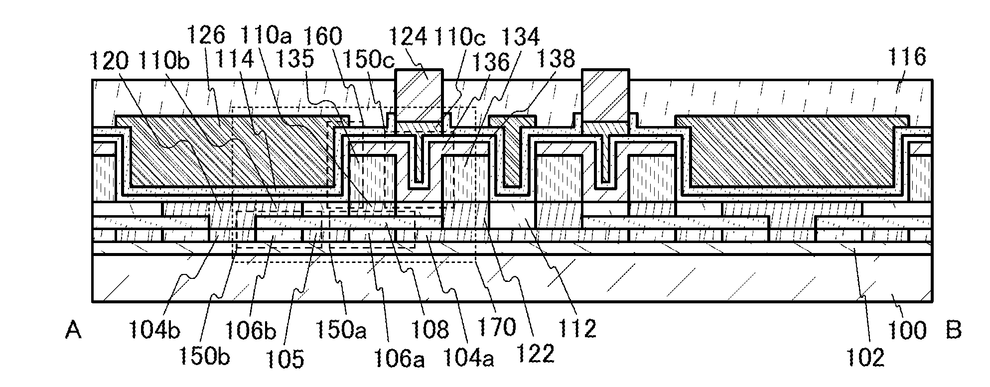
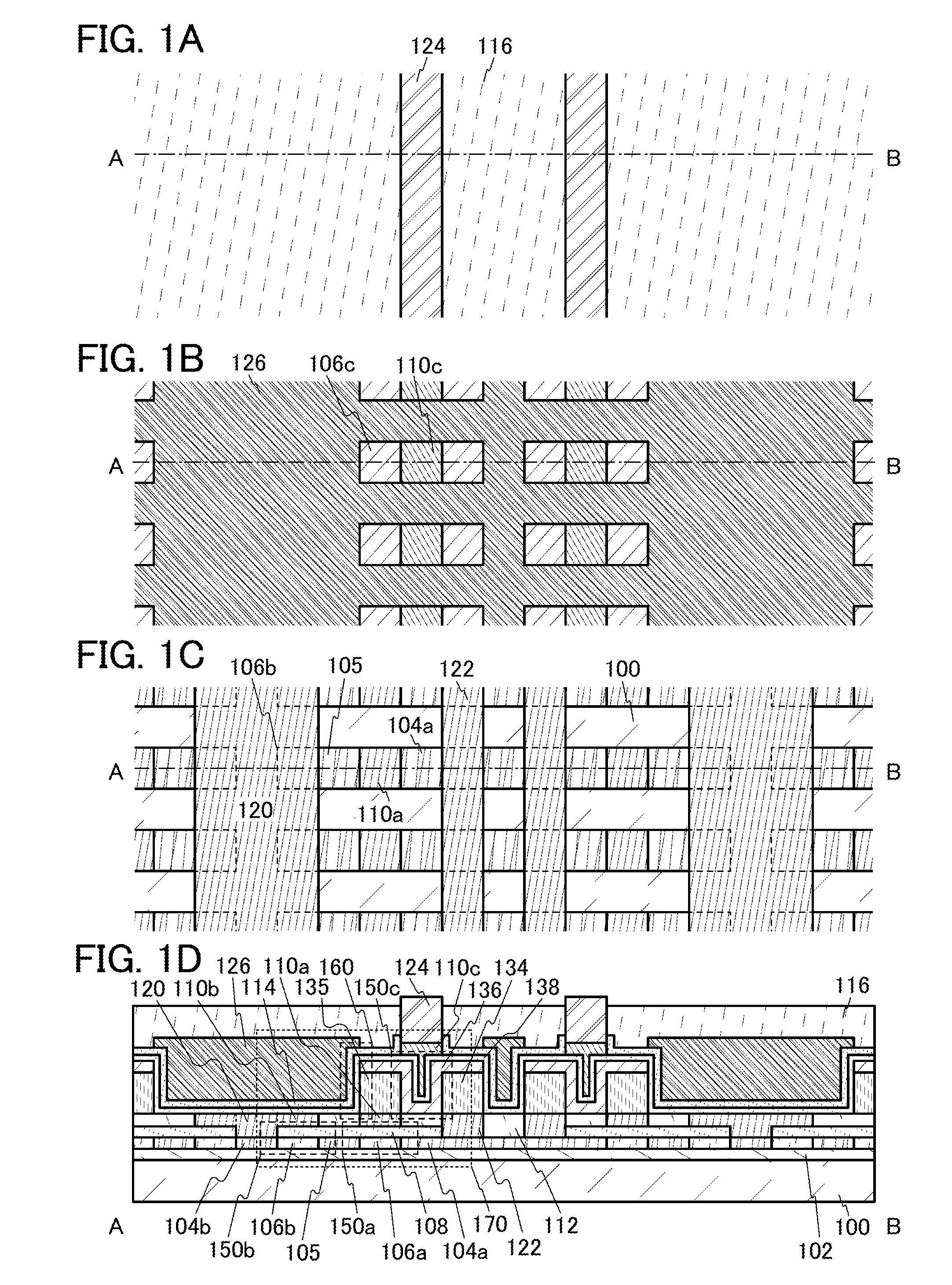
[0049]FIGS. 1A to 1C are top views illustrating parts of layers at respective levels of a memory cell array that is a semiconductor memory device. FIG. 1D illustrates a cross-section A-B corresponding to a dashed-dotted line A-B in FIGS. 1A to 1C. Note that FIG. 1A illustrates a layer at a level closer to a top surface, and FIG. 1C illustrates a layer at a level closer to a substrate 100. FIG. 1B illustrates a layer between the layers of FIGS. 1A and 1C. For simplification, some films (e.g., a first insulating film 102, a second insulating film 108, a third insulating film 112, a fourth insulating film 138, a fifth insulating film 114, and the like) are not illustrated in the top views.

[0050]The cross section A-B illustrated in FIG. 1D is described.

[0051]The memory cell array illustrated in FIG. 1D includes a memory cell 170 and a memory cell similar ...

embodiment 2

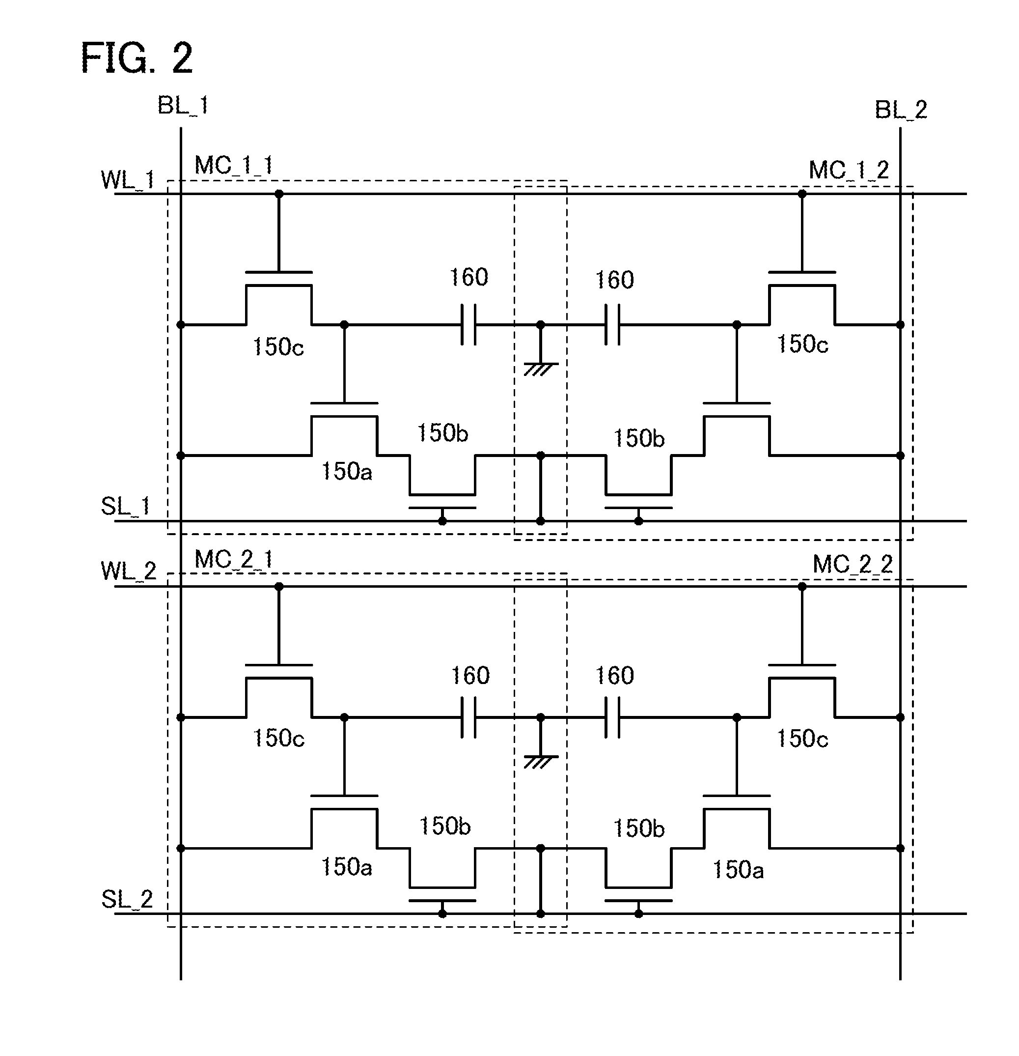
[0157]In this embodiment, a memory cell array including memory cells, which has a different structure from that described in Embodiment 1 will be described with reference to FIGS. 5A and 5B.

[0158]A memory cell 270 illustrated in FIG. 5A is different from the memory cell 170 in that a fourth insulating film 238 is provided only over an oxide semiconductor film 136. That is, the shape of a top surface of the fourth insulating film 238 substantially corresponds to the shape of a top surface of the oxide semiconductor film 136.

[0159]Since the fourth insulating film 238 is provided over only the oxide semiconductor film 136, a capacitor 260 has a different shape from the capacitor 160. Specifically, a netlike conductive film 226, the fourth insulating film 238, and a fifth insulating film 214 are provided without the netlike conductive film 126, the fourth insulating film 138, and the fifth insulating film 114.

[0160]Since the fourth insulating film 238 is provided over only the oxide sem...

embodiment 3

[0171]A central processing unit (CPU) can be formed using the semiconductor memory device described in Embodiment 1 or Embodiment 2 for at least part of the CPU.

[0172]FIG. 6A is a block diagram illustrating a specific structure of a CPU. The CPU illustrated in FIG. 6A includes an arithmetic logic unit (ALU)1191, an ALU controller 1192, an instruction decoder 1193, an interrupt controller 1194, a timing controller 1195, a register 1196, a register controller 1197, a bus interface (Bus I / F) 1198, a rewritable ROM 1199, and an ROM interface (ROM I / F) 1189 over a substrate 1190. A semiconductor substrate, an SOI substrate, a glass substrate, or the like is used as the substrate 1190. The ROM 1199 and the ROM interface 1189 may be provided over a separate chip. Obviously, the CPU illustrated in FIG. 6A is only an example in which the structure is simplified, and a variety of structures is applied to an actual CPU depending on the application.

[0173]An instruction that is input to the CPU ...


PUM

PropertyMeasurementUnit
temperaturesaaaaaaaaaa
thicknessaaaaaaaaaa
thicknessaaaaaaaaaa

Abstract

In the semiconductor memory device, one of a source and a drain of a first transistor is connected to one of a source and a drain of a second transistor, a gate of the first transistor is connected to one of a source and a drain of a third transistor and one of a pair of capacitor electrodes included in a capacitor, the other of the source and the drain of the first transistor and the other of the source and the drain of the third transistor are connected to a bit line, the other of the pair of capacitor electrodes included in the capacitor is connected to a common wiring, and the common wiring is grounded (GND). The common wiring has a net shape when seen from the above, and the third transistor is provided in a mesh formed by the common wiring.

Description

BACKGROUND OF THE INVENTION[0001]1. Field of the Invention[0002]The present invention relates to a semiconductor memory device which includes a circuit including a semiconductor element such as a transistor.[0003]2. Description of the Related Art[0004]Semiconductor memory devices are broadly classified into two categories: a volatile device that loses stored data when power supply stops, and a non-volatile device that retains stored data even when power is not supplied.[0005]A typical example of a volatile semiconductor memory device is a dynamic random access memory (DRAM). A DRAM stores data in such a manner that a transistor included in the semiconductor memory device is selected and charge is stored in a capacitor connected to the transistor.[0006]In a DRAM, since charge of a capacitor is lost instantaneously after information is read out, rewriting needs to be performed every time information is read out. In addition, when a transistor included in the DRAM is off, charge is los...

Claims


Application Information

Patent Timeline
Patent Type & Authority Applications(United States)
IPC IPC(8): H01L27/108
CPCH01L21/84H01L27/1156H01L27/1203H01L27/1225H01L28/60H01L27/10805H01L28/90H01L27/0288G11C11/405G11C16/0433H01L28/86H10B41/70H10B12/30
Inventor SAITO, TOSHIHIKO
Owner SEMICON ENERGY LAB CO LTD
Why Eureka
Try Eureka