Method for manufacturing semiconductor device

a semiconductor device and manufacturing method technology, applied in the field of semiconductor devices, can solve the problems of not being suitable for a larger glass substrate, and achieve the effect of stable electric characteristics and highly reliable semiconductor devices

Active Publication Date: 2012-03-15
SEMICON ENERGY LAB CO LTD
View PDF3 Cites 125 Cited by
  • Summary
  • Abstract
  • Description
  • Claims
  • Application Information

AI Technical Summary

Benefits of technology

[0057]A transistor, in which a channel region is included in a crystalline oxide semiconductor film having a hexagonal crystal structure where bonds for forming hexagonal lattices are formed in the a-b plane and c-axes are substantially perpendicular to a plan surface of a substrate which is substantially parallel to the a-b plane, is manufactured, whereby the amount of change in the threshold voltage of the transistor between befo

Problems solved by technology

On the other hand, although a transistor manufactured using polycrystalline silicon has high f

Method used


Image

  • Method for manufacturing semiconductor device
  • Method for manufacturing semiconductor device
  • Method for manufacturing semiconductor device

Examples


embodiment 1

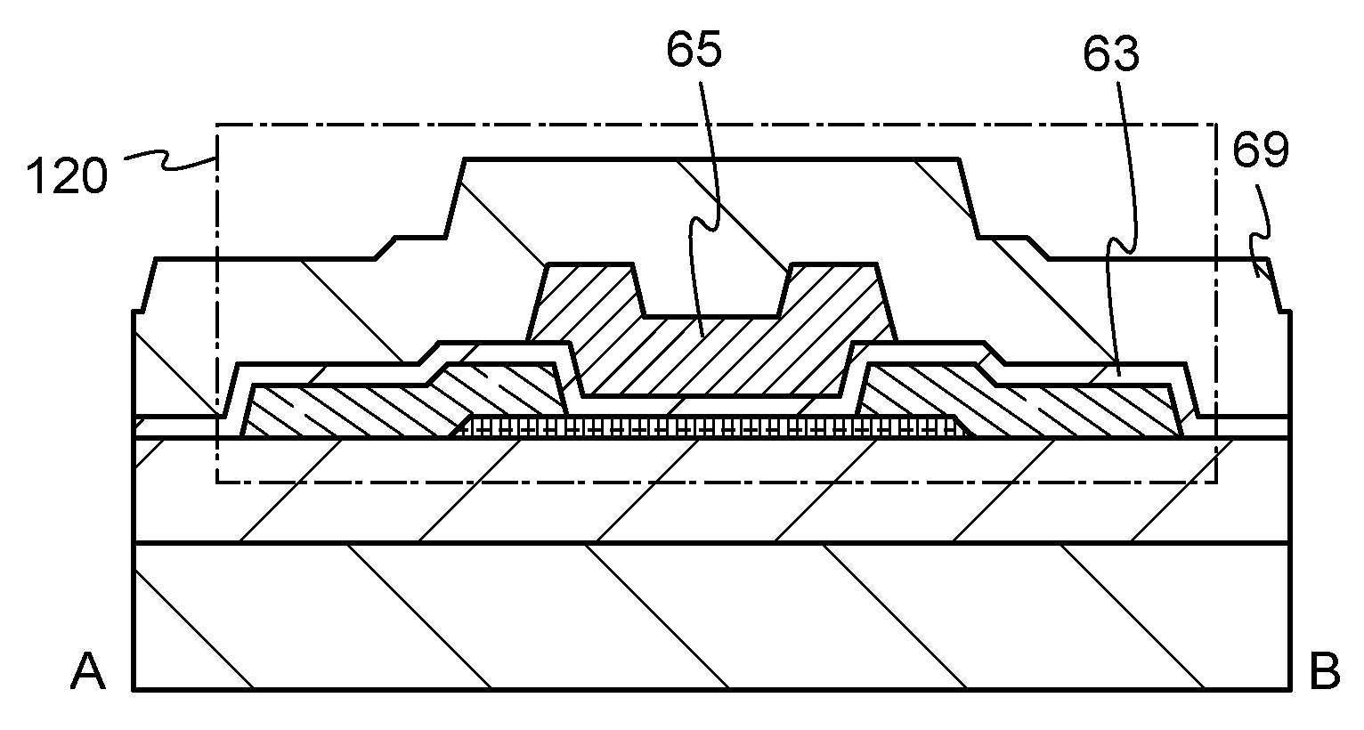
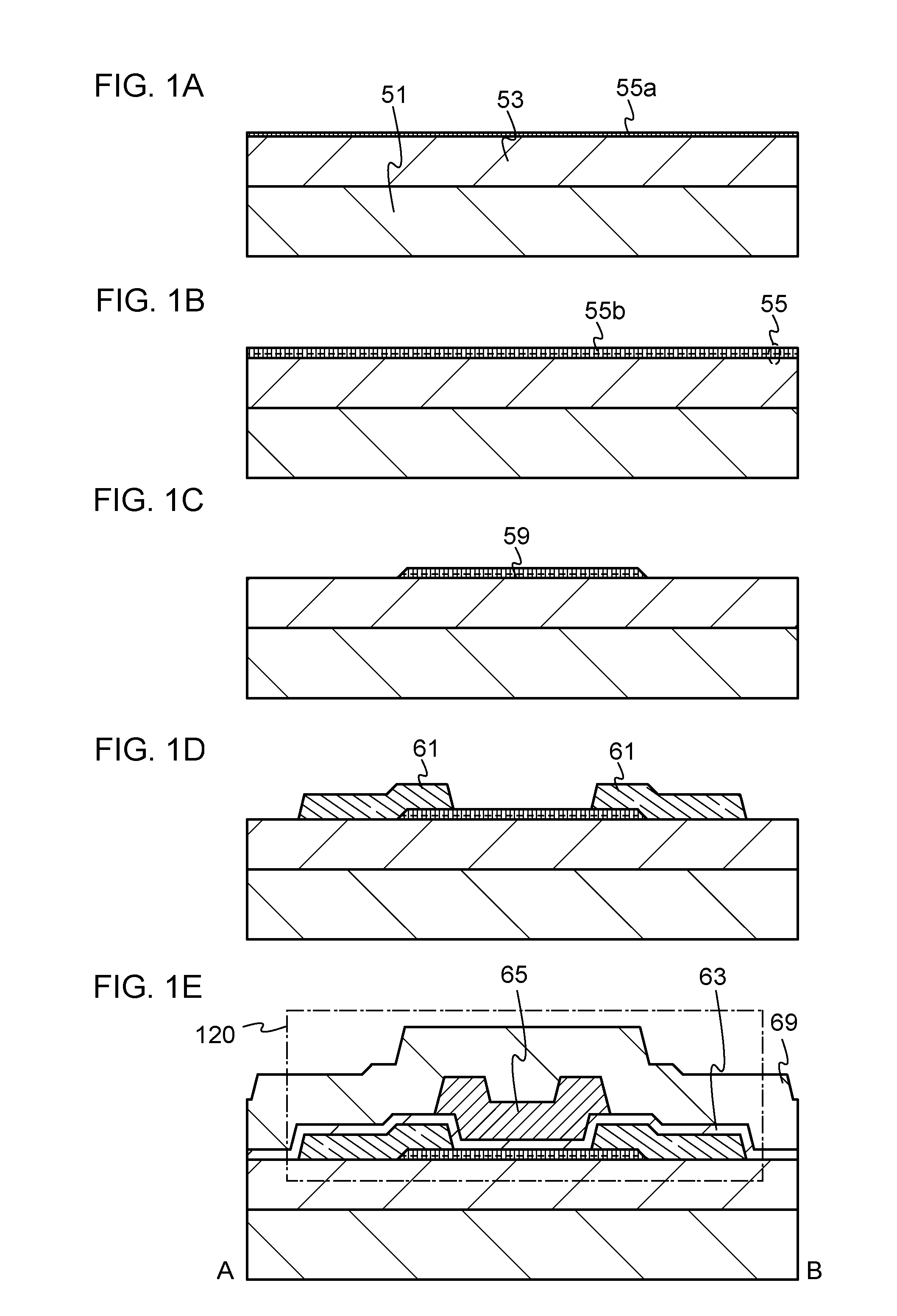
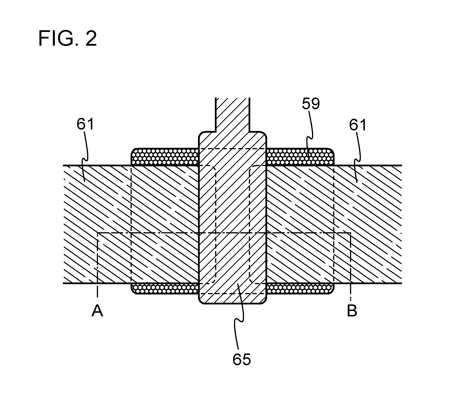
[0089]In this embodiment, a method for manufacturing a crystalline oxide semiconductor and a method for manufacturing a transistor including the crystalline oxide semiconductor will be described with reference to FIGS. 1A to 1E and FIG. 2. FIGS. 1A to 1E are cross-sectional views illustrating a manufacturing process of a transistor as one mode of a structure of a semiconductor device. The cross-sectional view taken along the dot-dash line A-B in FIG. 2 corresponds to FIG. 1E. In this embodiment, the transistor having a top gate structure is described.

[0090]As illustrated in FIG. 1A, an oxide insulating film 53 is formed over a substrate 51.

[0091]The substrate 51 should have at least heat resistance high enough to withstand heat treatment performed later. When a glass substrate is used as the substrate 51, a glass substrate whose strain point is higher than or equal to 730° C. is preferably used. As the glass substrate, for example, a glass material such as aluminosilicate glass, alu...

embodiment 2

[0171]In this embodiment, a manufacturing method of a transistor having a structure different from that in Embodiment 1 will be described with reference to FIGS. 5A to 5D and FIG. 6. The transistor in this embodiment is different from that in Embodiment 1 in that a pair of electrodes is provided between an oxide insulating film and a crystalline oxide semiconductor film. Note that the cross-sectional view taken along the dot-dash line C-D in FIG. 6 corresponds to FIG. 5D.

[0172]As illustrated in FIG. 5A, the oxide insulating film 53 is formed over the substrate 51 as in Embodiment 1. A pair of electrodes 71 is formed over the oxide insulating film 53. A crystalline oxide semiconductor film 73 is formed over the pair of electrodes 71 and the oxide insulating film 53.

[0173]The pair of electrodes 71 can be formed as appropriate by using a material and by a formation method which are similar to those of the pair of electrodes 61 described in Embodiment 1.

[0174]The crystalline oxide semic...

embodiment 3

[0184]In this embodiment, a transistor which is different from the transistors in Embodiment 1 and Embodiment 2 will be described with reference to FIGS. 7A to 7C and FIG. 8. The transistor in this embodiment has a bottom-gate structure in which a gate electrode is provided on the substrate side, which is different from the transistors in Embodiment 1 and Embodiment 2. Note that the cross-sectional view taken along the dot-dash line E-F in FIG. 8 corresponds to FIG. 7C.

[0185]As illustrated in FIG. 7A, the oxide insulating film 53 is formed over the substrate 51. A gate electrode 91 is formed over the oxide insulating film 53. A gate insulating film 93 is formed over the oxide insulating film 53 and the gate electrode 91. Then, a crystalline oxide semiconductor film 95 is formed over the gate insulating film 93 as in Embodiment 1.

[0186]The gate electrode 91 can be formed in a manner similar to that of the gate electrode 65 in Embodiment 1.

[0187]The gate insulating film 93 can be form...


PUM


Abstract

An object is to manufacture a semiconductor device including an oxide semiconductor film, which has stable electric characteristics and high reliability. A crystalline oxide semiconductor film is formed, without performing a plurality of steps, as follows: by utilizing a difference in atomic weight of plural kinds of atoms included in an oxide semiconductor target, zinc with low atomic weight is preferentially deposited on an oxide insulating film to form a seed crystal including zinc; and tin, indium, or the like with high atomic weight is deposited on the seed crystal while causing crystal growth. Further, a crystalline oxide semiconductor film is formed by causing crystal growth using a seed crystal with a hexagonal crystal structure including zinc as a nucleus, whereby a single crystal oxide semiconductor film or a substantially single crystal oxide semiconductor film is formed.

Description

TECHNICAL FIELD[0001]An embodiment of the present invention relates to a semiconductor device which includes a circuit including at least a semiconductor element such as a transistor as an element, and a manufacturing method thereof. For example, embodiments of the present invention relate to an electronic device which includes, as a component, any of a power device mounted in a power circuit, a semiconductor integrated circuit including a memory, a thyristor, a converter, an image sensor, or the like, an electro-optical device typified by a liquid crystal display device, and a light-emitting display device including a light-emitting element.[0002]Note that the semiconductor device in this specification refers to all devices that can function by utilizing semiconductor characteristics, and electro-optic devices, semiconductor circuits, and electronic appliances are all semiconductor devices.BACKGROUND ART[0003]Transistors formed over a glass substrate or the like are typically manuf...

Claims


Application Information

Patent Timeline
IPC IPC(8): H01L21/44H05B44/00
CPCH01L29/7869H01L29/66969H01L23/564H01L23/552H01L2924/0002H01L2924/00H01L21/208H01L21/18H01L21/20H01L29/78606H01L29/04H01L29/78696
Inventor YAMAZAKI, SHUNPEINONAKA, YUSUKEINOUE, TAKAYUKITSUBUKU, MASASHIAKIMOTO, KENGOMIYANAGA, AKIHARU
Owner SEMICON ENERGY LAB CO LTD
Why Eureka
Try Eureka