

Semiconductor device with floating gate and electrically floating body
a technology which is applied in the field of magnetic gate and floating body, can solve the problems power consumption, memory availability, and power consumption, and achieving the effects of increasing memory die area, increasing power consumption, and increasing memory die area
- Summary
- Abstract
- Description
- Claims
- Application Information
AI Technical Summary
Benefits of technology
Problems solved by technology
Method used
Image

Examples
Embodiment Construction
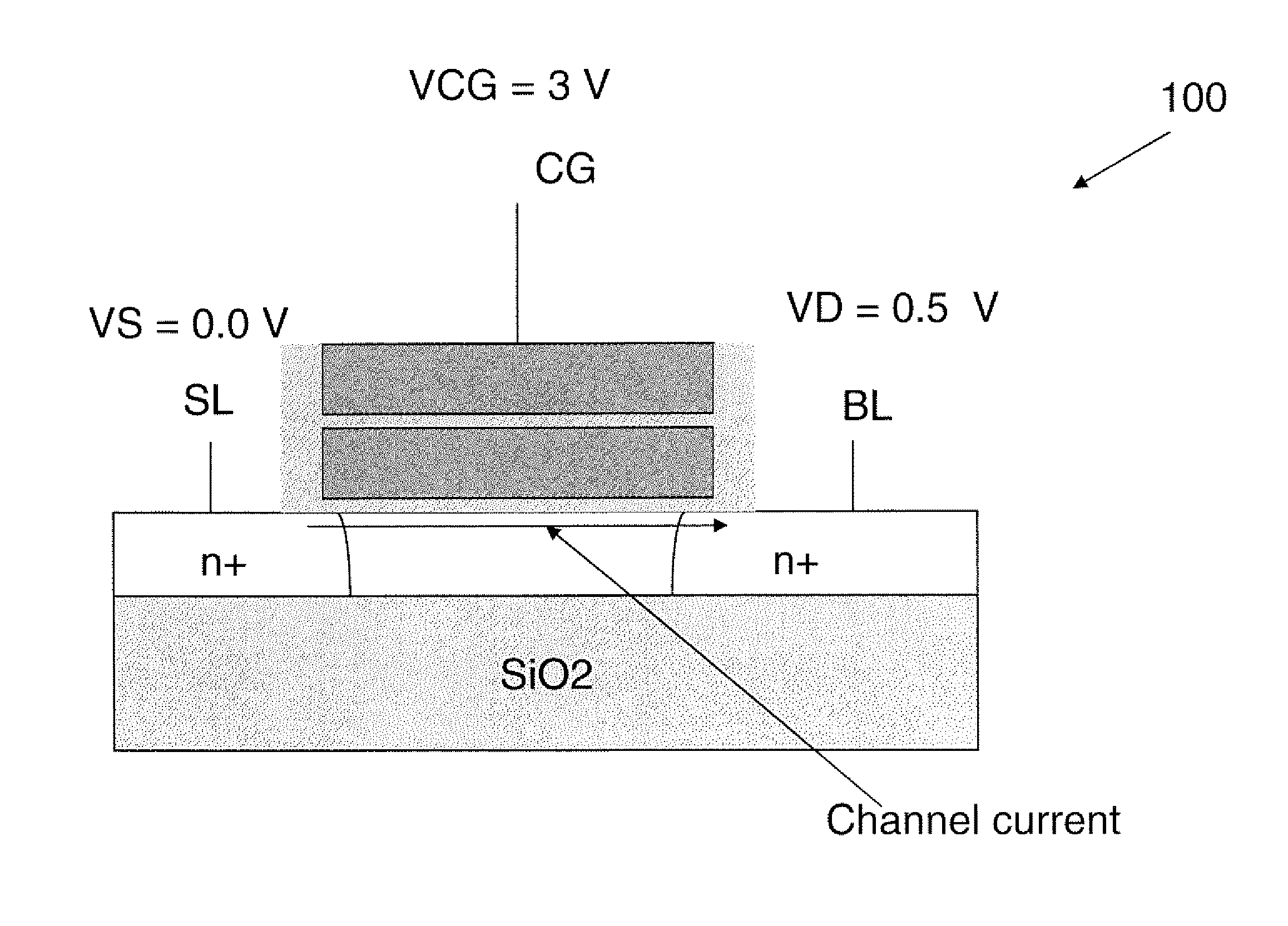
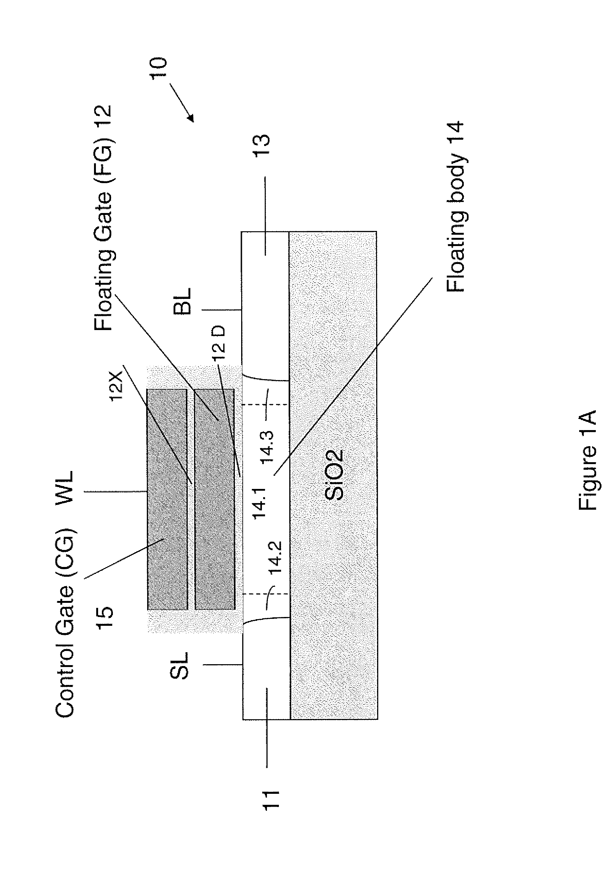
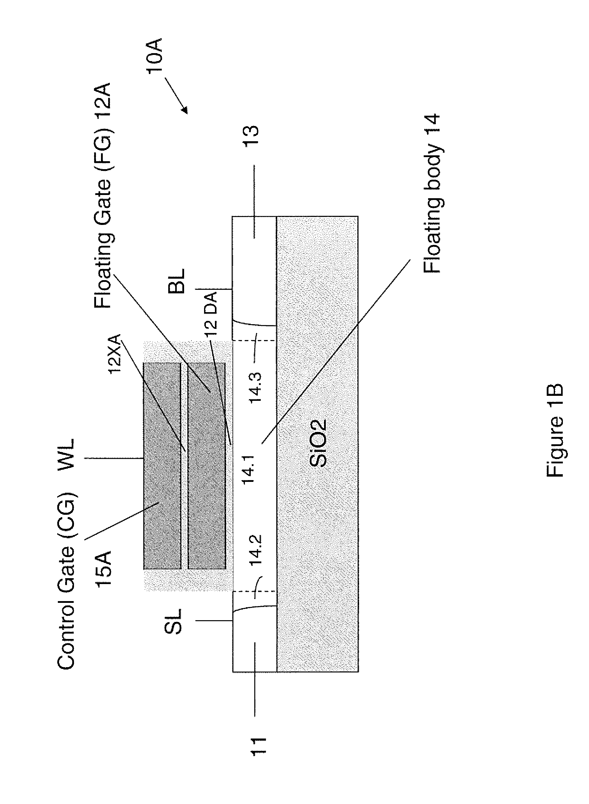
[0037]There are many aspects of the present disclosure described herein as well as many embodiments of those aspects. In one aspect, the present disclosure may be directed to a semiconductor device including a floating gate and an electrically floating body. In another aspect, the present disclosure may be directed to techniques to control and / or operate a semiconductor memory cell (and memory cell array having a plurality of such memory cells as well as an integrated circuit device including a memory cell array) having one or more transistors having a floating gate and an electrically floating body in which an electrical charge is stored in the floating gate or the electrically floating body (according to the mode of operation of the transistor).
[0038]The present disclosure may also be directed to semiconductor memory cells, arrays, circuitry and devices to implement such control and operation techniques. Notably, the memory cell and / or memory cell array may comprise a portion of a...
PUM
 Abstract
Description
Claims
Application Information