Method of decomposing layout of semiconductor device and method of manufacturing semiconductor device using the same

a semiconductor device and layout technology, applied in the direction of cad circuit design, computer aided design, instruments, etc., can solve the problems of increasing the loading effect and affecting the uniformity of the critical dimension, and achieve the effect of reducing the difference between the density of the pattern

Active Publication Date: 2016-03-10
SAMSUNG ELECTRONICS CO LTD
View PDF0 Cites 3 Cited by
  • Summary
  • Abstract
  • Description
  • Claims
  • Application Information

AI Technical Summary

Benefits of technology

[0008]Example embodiments relate to a method of decomposing a layout of a semiconductor device that effectively reduces a difference between pattern densities of a plurality of decomposed patterns.

Problems solved by technology

However, when pattern densities of the plurality of decomposed patterns are different from each other, a critical dimension uniformity may be affected and a loading effect may increase while performing a mask manufacturing process and an etching process based on the plurality of decomposed patterns.

Method used


Image

  • Method of decomposing layout of semiconductor device and method of manufacturing semiconductor device using the same
  • Method of decomposing layout of semiconductor device and method of manufacturing semiconductor device using the same
  • Method of decomposing layout of semiconductor device and method of manufacturing semiconductor device using the same

Examples


Embodiment Construction

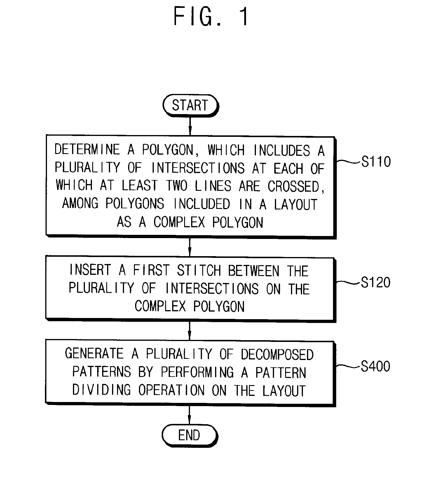
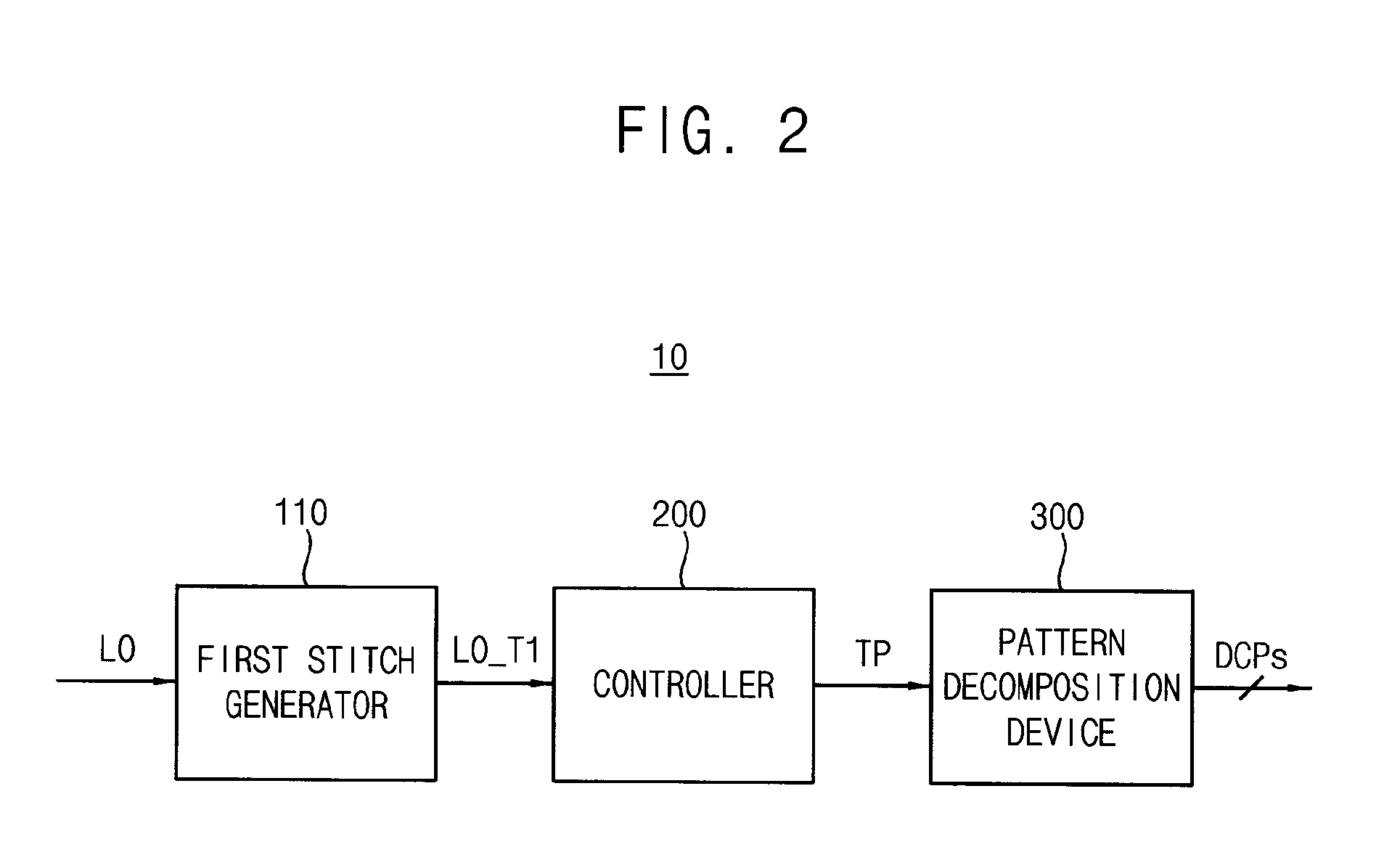
[0068]Example embodiments will now be described more fully with reference to the accompanying drawings, in which some example embodiments are shown. Example embodiments, may, however, be embodied in many different forms and should not be construed as being limited to the embodiments set forth herein; rather, these example embodiments are provided so that this disclosure will be thorough and complete, and will fully convey the scope of example embodiments of inventive concepts to those of ordinary skill in the art. In the drawings, the thicknesses of layers and regions are exaggerated for clarity. Like reference characters and / or numerals in the drawings denote like elements, and thus their description may be omitted.

[0069]Spatially relative terms, such as “beneath,”“below,”“lower,”“above,”“upper” and the like, may be used herein for ease of description to describe one element or feature's relationship to another element(s) or feature(s) as illustrated in the figures. It will be unde...


PUM


Abstract

In a method of decomposing a layout of a semiconductor device, a polygon, which includes a plurality of intersections at each of which at least two lines are crossed, among polygons included in the layout of the semiconductor device may be determined as a complex polygon. A first stitch may be inserted between the plurality of intersections on the complex polygon. A plurality of decomposed patterns may be generated by performing a pattern dividing operation on the layout.

Description

CROSS-REFERENCE TO RELATED APPLICATION(S)[0001]This application claims priority under 35 USC §119 to Korean Patent Application No. 10-2014-0117785, filed on Sep. 4, 2014 in the Korean Intellectual Property Office (KIPO), the contents of which are herein incorporated by reference in their entirety.BACKGROUND[0002]1. Technical Field[0003]Example embodiments relate to a method of manufacturing a semiconductor device, and more particularly to a method of decomposing a layout of a semiconductor device.[0004]2. Description of Related Art[0005]In manufacturing a high density semiconductor device, a double patterning technology (DPT) process is generally used to avoid a conflict between patterns included in a layout of the semiconductor device. In the DPT process, a layout of a semiconductor device is decomposed into two patterns, and a wiring pattern is formed on a substrate by performing a lithography process on the substrate two times using the two patterns.[0006]Recently, a triple patte...

Claims


Application Information

Patent Timeline
Patent Type & Authority Applications(United States)
IPC IPC(8): G06F17/50H01L21/311H01L21/768
CPCG06F17/5068H01L21/31144H01L21/768G06F30/39G06F30/398H01L21/0274H01L21/76816
Inventor KANG, DAE-KWONJUNG, JI-YOUNGKIM, DONG-GYUNYANG, JAE-SEOKHWANG, SUNG-WOOK
Owner SAMSUNG ELECTRONICS CO LTD
Why Eureka
Try Eureka