Semiconductor Device, Driver IC, Display Device, and Electronic Device

a technology of semiconductor devices and driver ics, applied in the field of semiconductor devices, can solve the problems of reducing the display quality of the display device, and it is extremely difficult to completely match the electrical characteristics of the driving transistor in a large number of pixels, and achieve the effect of high accuracy

Active Publication Date: 2016-03-10
SEMICON ENERGY LAB CO LTD
View PDF2 Cites 27 Cited by
  • Summary
  • Abstract
  • Description
  • Claims
  • Application Information

AI Technical Summary

Benefits of technology

[0021]One embodiment of the present invention can provide a novel semiconductor device or a method for operating the novel semiconductor device. Alternatively, one embodiment of the present invention can miniaturize a semiconductor device or verify the operation with high accuracy.
[0022]Note that the description of the plurality of effects does not distur

Problems solved by technology

The variation in the electrical characteristics of the driving transistor between a plurality of pixels is a cause of a reduction in the display qualit

Method used


Image

  • Semiconductor Device, Driver IC, Display Device, and Electronic Device
  • Semiconductor Device, Driver IC, Display Device, and Electronic Device
  • Semiconductor Device, Driver IC, Display Device, and Electronic Device

Examples


embodiment 1

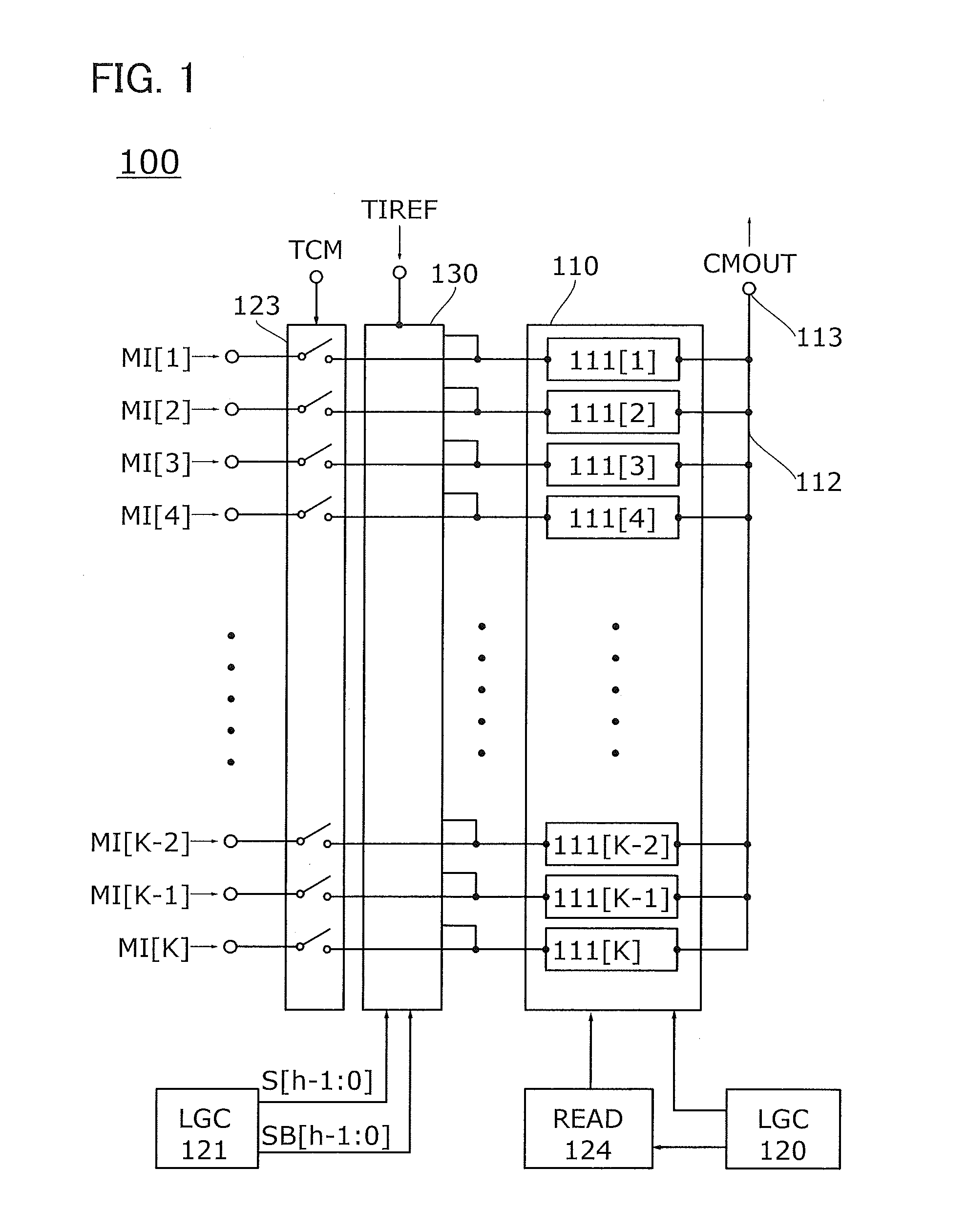
[0053]A semiconductor device including a pass transistor logic circuit is described. Here, an example in which the pass transistor logic circuit is used in a test circuit for verifying the operation of a circuit is shown.

[0054]A semiconductor device 100 illustrated in FIG. 1 includes a circuit 110, a wiring 112, an output terminal 113, a logic circuit (LGC) 120, a logic circuit (LGC) 121, a switch circuit 123, a read circuit (READ) 124, and a pass transistor logic circuit (PTL) 130. The circuit 110 includes K-stage circuits 111 (K is an integer of 2 or more). The semiconductor device 100 further includes K input terminals and an output terminal which outputs a signal CMOUT. Signals MI[1] to MI[K] are input to the respective K input terminals.

[0055]The switch circuit 123 has a function of controlling the input of the signals MI[1] to MI[K] to the circuit 110. The switch circuit 123 includes K switches. Each switch controls the electrical continuity between the circuit 110 and any one...

embodiment 2

[0067]Here, a display device is described as an example of the semiconductor device including the pass transistor logic circuit. An example in which the semiconductor device in Embodiment 1 is provided in a driver circuit is described.

Display Device

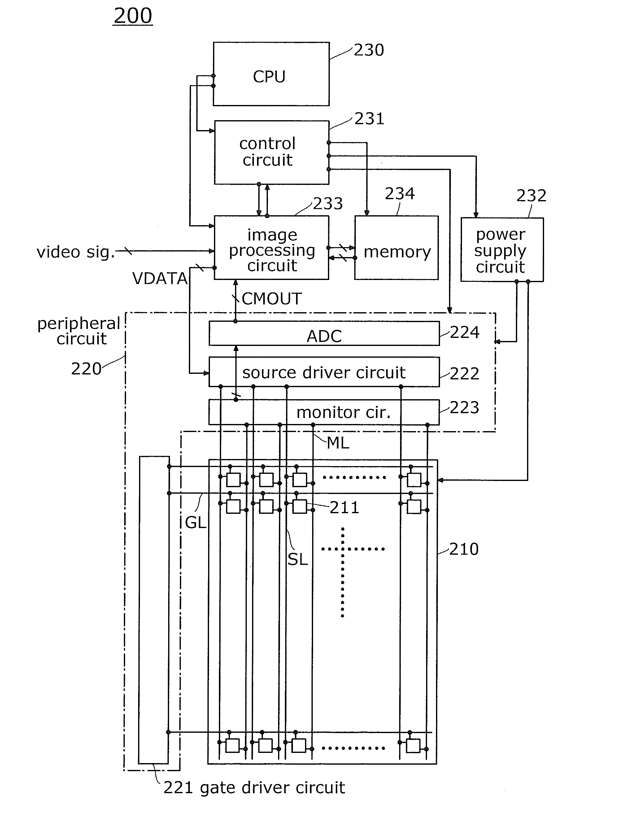
[0068]FIG. 5 is a block diagram illustrating a configuration example of a display device. The display device 200 includes a pixel portion 210, a peripheral circuit 220, a CPU 230, a control circuit 231, a power supply circuit 232, an image processing circuit 233, and a memory 234.

[0069]The CPU 230 is a circuit for executing an instruction and controlling the display device 200 collectively. The CPU 230 executes an instruction input from the outside and an instruction stored in an internal memory. The CPU 230 generates signals for controlling the control circuit 231 and the image processing circuit 233. On the basis of a control signal from the CPU 230, the control circuit 231 controls the operation of the display device 200. The control c...

operation example

[0089]The data signal Vda is input to the wiring SL. The voltage value of the data signal Vda corresponds to the gray scale of the video signal. In FIG. 8B, Vda[k] and Vda[k+1] represent the data signals Vda input to the k-th pixel 211 and the (k+1)-th pixel 211, respectively.

[0090]A period P1 is a writing operation period and the light-emitting element EL1 does not emit light during the period. Voltage Vano is applied to the wiring ANL and voltage Vcat is applied to the cathode of the light-emitting element EL1. The wiring ML is electrically connected to a power supply line supplying voltage V0. The wiring GL is set at a high level to turn on the transistors M1 and M3. The voltage of the wiring SL is applied to the node N2, so that the drain current having a value corresponding to the voltage flows in the transistor M2.

[0091]Note that the voltage Vano, the voltage V0, and the voltage Vcat are preferably set so as to satisfy the following formulae (b1), (b2), and (b3). In the follow...


PUM


Abstract

A semiconductor device including a test circuit is miniaturized. The semiconductor device includes r first input terminals (r is an integer of 2 or more), a second input terminal, r functional circuits, a demultiplexer, and a switch circuit. The demultiplexer is a pass transistor logic circuit. R output terminals of the demultiplexer are electrically connected to respective input terminals of the functional circuit and the input terminal is electrically connected to the second input teiminal. Input terminals of the r circuits are electrically connected to the respective first input terminals through the switch circuit. For example, a signal for verification is input to the first input terminal in verification of the functional circuit to operate the demultiplexer. One signal for verification is input to r functional circuits by the demultiplexer.

Description

TECHNICAL FIELD[0001]One embodiment of the present invention relates to a circuit, a processing circuit, or a storage circuit including a semiconductor; a semiconductor device such as a display device or a light-emitting device; a driving method thereof; a manufacturing method thereof; or the like.BACKGROUND ART[0002]As for pixels of active matrix display devices using light-emitting elements, a variety of circuit configurations are proposed. In general, a pixel is provided with at least a light-emitting element, a transistor which controls input of a data signal to the pixel, and a transistor which controls a current supplied to the light-emitting element (driving transistor). Supplying a drain current flowing in the driving transistor to the light-emitting element makes the light-emitting element emit light at a luminance corresponding to the drain current value. The drain current of the driving transistor is controlled by the voltage of a data signal.[0003]Therefore, when there i...

Claims


Application Information

Patent Timeline
IPC IPC(8): G09G3/32H01L27/32H01L29/786H03K17/00
CPCG09G3/3275H01L29/7869H01L27/3276G09G2310/0297H03K17/007G09G3/3225G09G2310/027H01L27/3262G09G3/3291G09G2300/0842G09G2300/0861G09G2310/0262G09G2320/0295H01L27/1225H10K59/1213H10K59/131
Inventor TAKAHASHI, KEIKOBAYASHI, HIDETOMO
Owner SEMICON ENERGY LAB CO LTD
Why Eureka
Try Eureka