

Liquid crystal panel, liquid crystal display device including liquid crystal panel, and method of manufacturing liquid crystal panel
a liquid crystal display and liquid crystal technology, applied in semiconductor devices, instruments, optics, etc., can solve the problems of cost increase, reduction in light efficiency, and reduction in light efficiency, and achieve the effect of preferable viewing angle characteristics
- Summary
- Abstract
- Description
- Claims
- Application Information
AI Technical Summary
Benefits of technology
Problems solved by technology
Method used
Image

Examples
first preferred embodiment
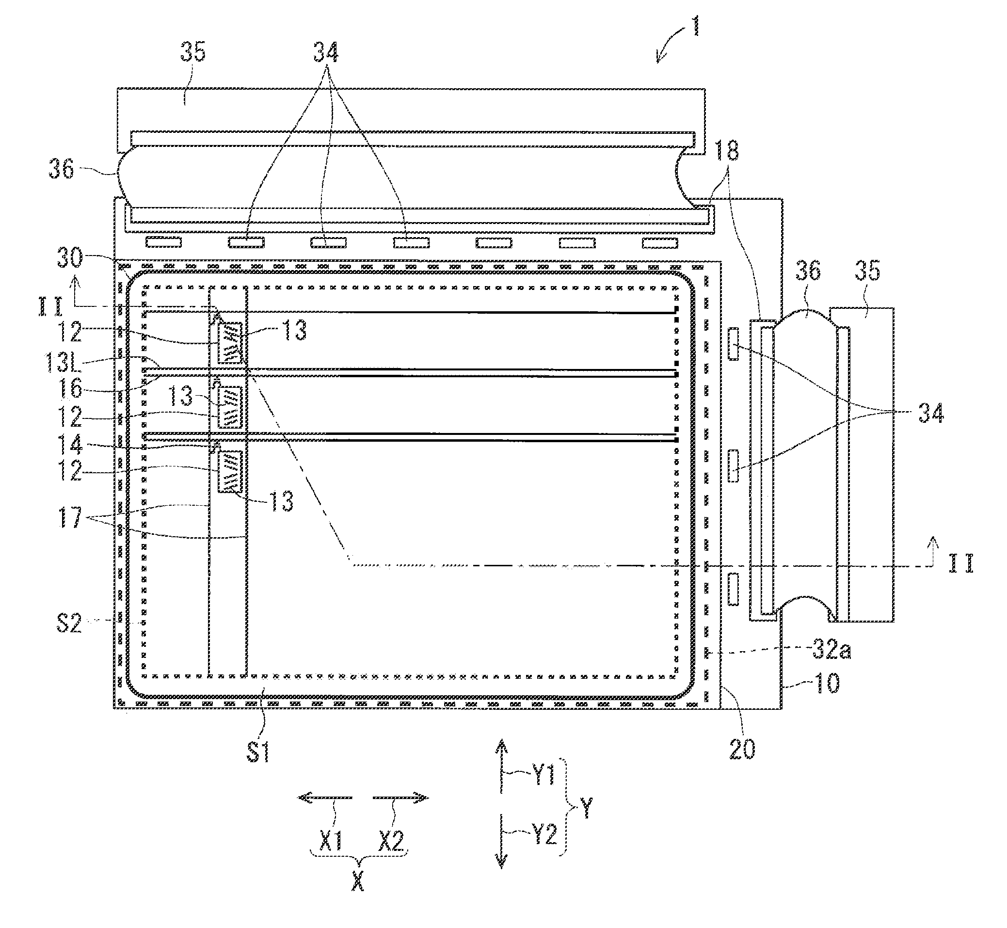
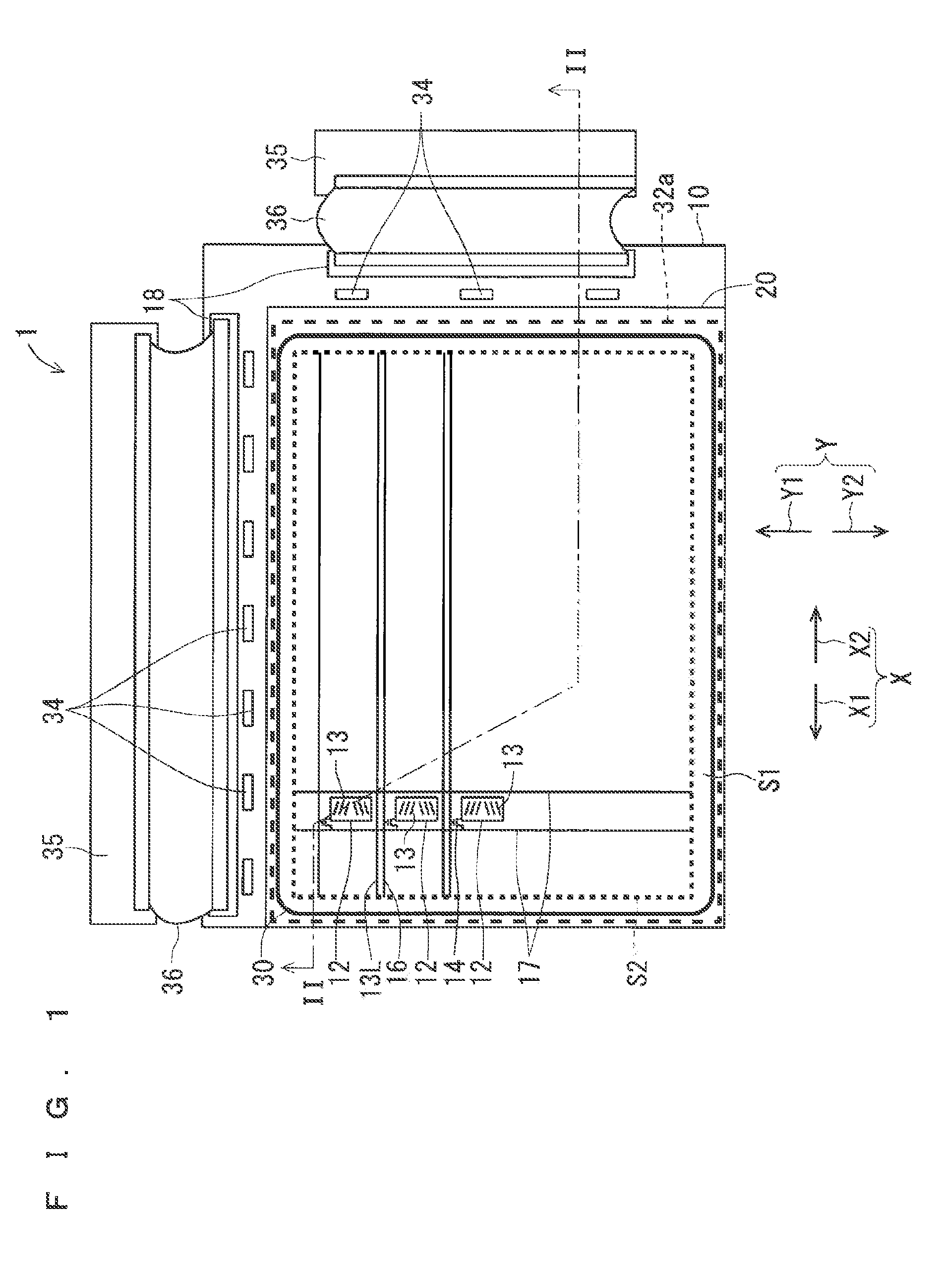
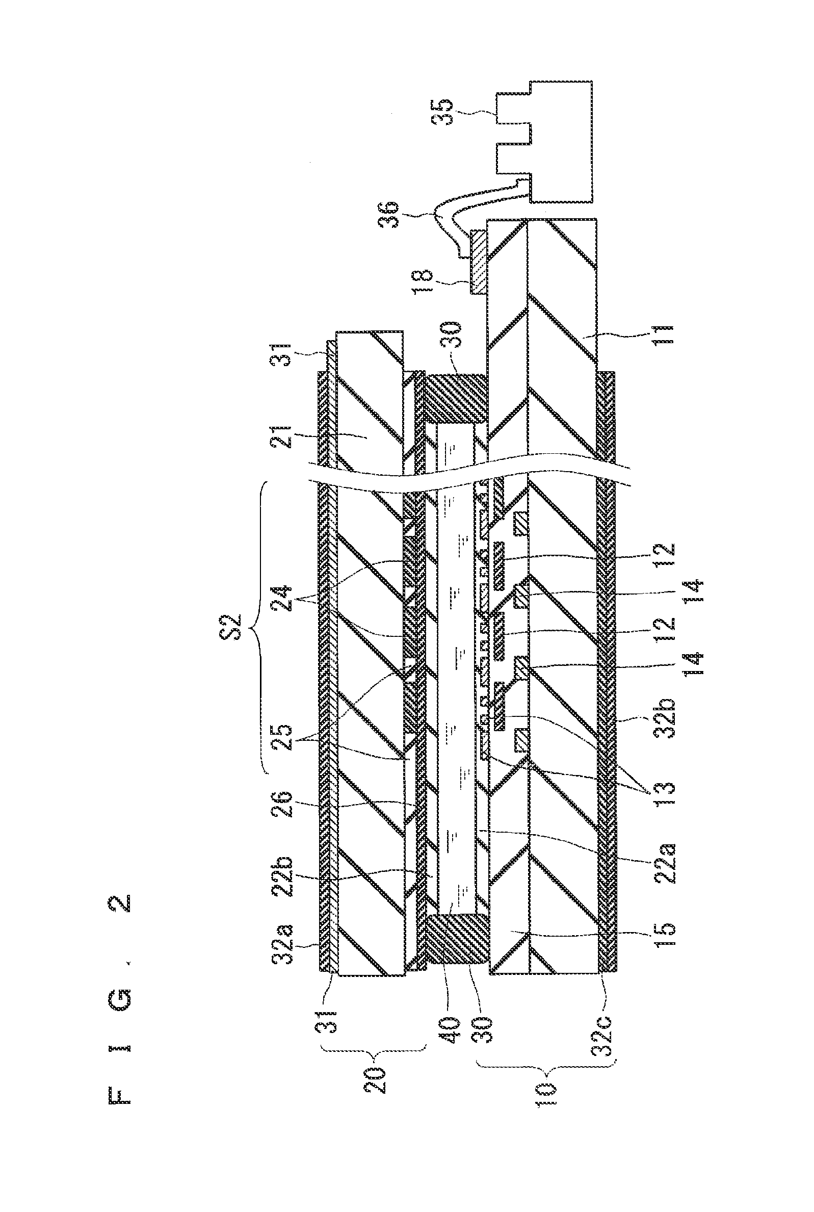
[0064]FIG. 1 is a plan view showing the structure of a liquid crystal panel 1 provided in a liquid crystal display device according to a first preferred embodiment of the present invention. FIG. 2 is a sectional view of the liquid crystal panel 1 as viewed from a cutting plane line II-II of FIG. 1.
[0065]The liquid crystal panel 1 shown as an example in FIGS. 1 and 2 adopts an in-plane system operated by using a thin film transistor (abbreviated as TFT) as a switching element. The liquid crystal panel 1 is more specifically a liquid crystal panel adopting a fringe field switching (FFS) system.
[0066]As shown in FIGS. 1 and 2, the liquid crystal panel 1 includes a TFT array substrate (simply called an “array substrate” in some cases) 10, a color filter substrate 20, and a seal material 30.
[0067]Both the array substrate 10 and the color filter substrate 20 are quadrilateral, more specifically rectangular in outer shape. In the first preferred embodiment, the outer shape of the array sub...
second preferred embodiment
[0134]FIG. 8 shows an example of arrangement of optical components of a liquid crystal panel according to a second preferred embodiment of the present invention. The liquid crystal panel of the second preferred embodiment is similar to that of the first preferred embodiment. A structure same as that of the first preferred embodiment is identified by the same reference sign and description common to these structures will not be given repeatedly. In the second preferred embodiment, the direction of the slit portion of the slit electrode, the alignment direction of the liquid crystal molecule 41, the directions of the absorption axes 51 and 54 of the polarizing plates 32a and 32 respectively, and the direction of the delay phase axis 53 of the biaxial phase difference film 32c are the same as those of the first preferred embodiment. Like in the first preferred embodiment, a slit electrode of the second preferred embodiment is the counter electrode 13.
[0135]Like in the first preferred e...
third preferred embodiment
[0143]FIG. 10 shows an example of arrangement of optical components of a liquid crystal panel according to a third preferred embodiment of the present invention. The liquid crystal panel of the third preferred embodiment is similar to those of the first and second preferred embodiments. A structure same as that of the first and second preferred embodiments is identified by the same reference sign and description common to these structures will not be given repeatedly. In the third preferred embodiment, a direction of the slit portion of the slit electrode, the alignment direction of the liquid crystal molecule 41, the direction of the absorption axis 54 of the array substrate polarizing plate 32b, and the direction of the delay phase axis 53 of the biaxial phase difference film 32c are the same as those of the first and second preferred embodiments. Like in the first preferred embodiment, a slit electrode of the third preferred embodiment is the counter electrode 13.
[0144]Like in th...
PUM
 Abstract
Description
Claims
Application Information