Eureka AIR delivers breakthrough ideas for toughest innovation challenges, trusted by R&D personnel around the world.

Array substrate, display panel and display device

Active Publication Date: 2016-04-14
SHANGHAI TIANMA MICRO ELECTRONICS CO LTD +1
View PDF11 Cites 33 Cited by
  • Summary
  • Abstract
  • Description
  • Claims
  • Application Information

AI Technical Summary

Benefits of technology

The patent is about a new arrangement of touch electrodes in a display panel that reduces resistance and improves charging time. The touch electrodes are designed in a grid shape, and the first and second sub-electrodes are positioned between adjacent pixel electrodes. This reduces the resistance of the touch electrodes and the load capacitance between them and the source electrode, resulting in quicker charging of touch driving signals and better operational timing for touch and display.

Problems solved by technology

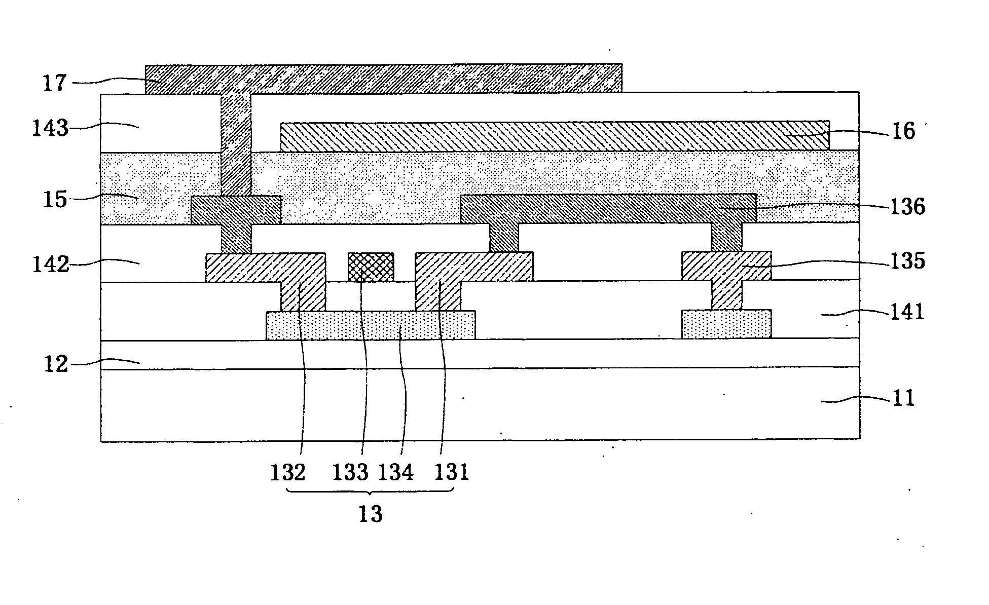
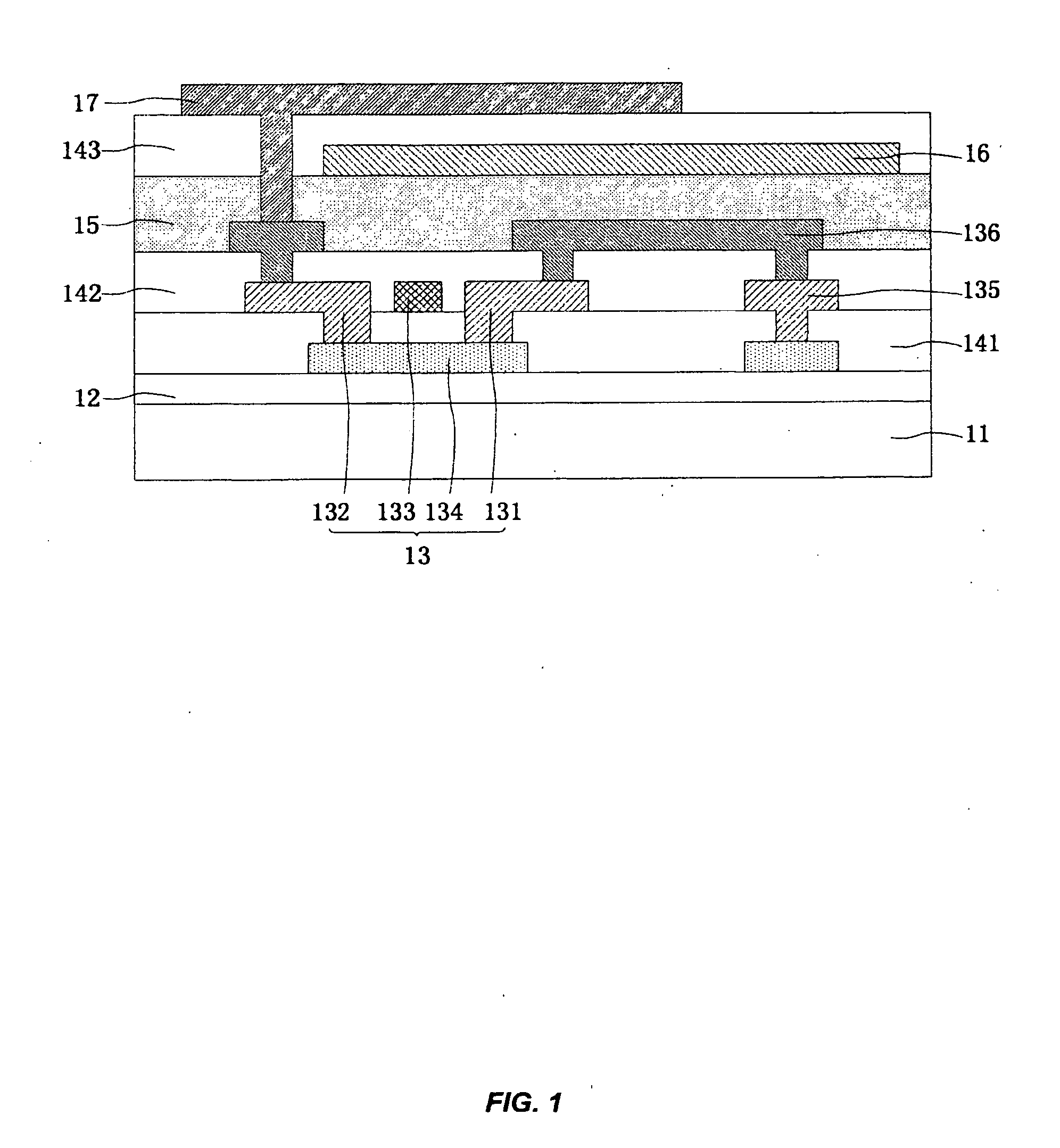
Moreover, the overlapping area between the source electrode 131 of the TFT 13 as well as the first metal 136 and the common electrode 16 is large, so that a large load capacitance is formed, and hence, the product of the load capacitance and resistance of the touch electrode is large, resulting in a long charging time of the touch driving signal, so that there is insufficient time available for the touch state and the display state to operate in a time division manner.

Method used


Image

  • Array substrate, display panel and display device
  • Array substrate, display panel and display device
  • Array substrate, display panel and display device

Examples


Embodiment Construction

[0026]The present disclosure will be further described in detail below in conjunction with the accompanying drawings and embodiments. It is to be understood that specific embodiments described herein are merely for explaining the present disclosure rather than limiting the present disclosure. Additionally, it is noted that merely partial contents associated with the present disclosure rather than all contents are illustrated in the accompanying drawings for ease of description.

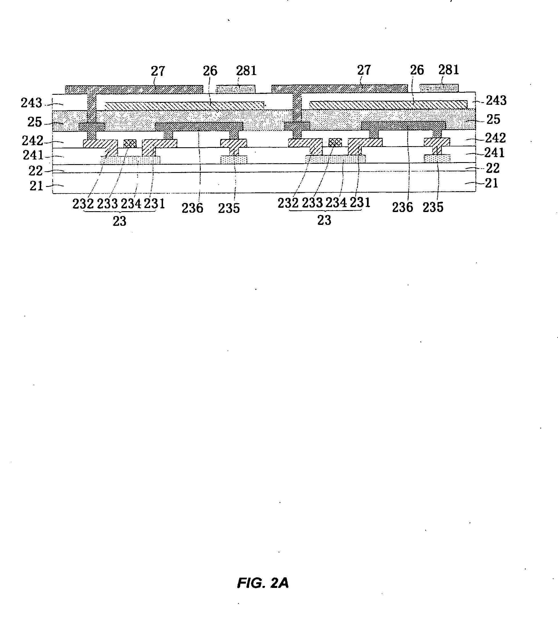
[0027]FIG. 2A is a schematic diagram of a structure of an array substrate according to an embodiment of the disclosure. As shown inFIG. 2A, the array substrate includes: a plurality of data lines 235; a plurality of scanning lines (not shown in FIG. 2A) which intersect the plurality of data lines 235 to define pixel units (not shown in FIG. 2A); pixel electrodes 27 disposed within the pixel units; and a plurality of touch electrodes, each of which has a grid shape and is formed by a plurality of first sub-elec...


PUM


Abstract

An array substrate includes a plurality of data lines; a plurality of scanning lines intersecting the data lines to define pixel units; a plurality of pixel electrodes within the pixel units; and a plurality of touch electrodes having a grid shape and formed by a plurality of first sub-electrodes and a plurality of second sub-electrodes intersecting each other. Projections of the first sub-electrodes and the second sub-electrodes onto a layer containing the pixel electrodes are respectively located between adjacent pixel electrodes, or the first sub-electrodes and the second sub-electrodes are respectively located between adjacent pixel electrodes. The product of the resistance of the touch electrode and the load capacitance between the touch electrode, the source electrode and the first metal is reduced, which reduces the charging time of the touch driving signal and enables the touch state and the display state to operate in a time division manner.

Description

CROSS-REFERENCES TO RELATED APPLICATIONS[0001]This application claims the benefit of priority to Chinese Patent Application No. 201410531586.4, filed with the Chinese Patent Office on Oct. 10, 2014 and entitled “ARRAY SUBSTRATE, DISPLAY PANEL AND DISPLAY DEVICE”, the content of which is incorporated herein by reference in its entirety.TECHNICAL FIELD[0002]The disclosure relates to the field of display technologies, in particular to an array substrate, a display panel and a display device.BACKGROUND OF THE INVENTION[0003]With the development of modern electronic technology, components for achieving functions such as capacitive touch functions are disposed on a display panel device to bring convenience to users.[0004]Nowadays, depending on the implementation, the capacitive touch function may be implemented as a self-capacitive touch function or a mutual-capacitive touch function. The self-capacitive touch function refers to a touch function achieved by capacitance formed between a to...

Claims


Application Information

Patent Timeline
IPC IPC(8): G06F3/041G02F1/1333G06F3/044
CPCG06F3/0416G06F2203/04112G02F1/13338G06F3/044G02F1/134309G02F1/136286G02F2201/12G06F3/0412G06F3/0488G06F3/0443G02F1/134372
Inventor LU, FENGHUANG, ZHONGSHOUZHANG, XIANXIANGLI, XIAOYELIU, GANGXU, YINGYING
Owner SHANGHAI TIANMA MICRO ELECTRONICS CO LTD
Why Eureka
Eureka Blog
Learn More