Group III nitride LED with undoped cladding layer and multiple quantum well

a nitride led, undoped technology, applied in the direction of semiconductor lasers, lasers, solid-state devices, etc., can solve the problems of less likely transition, less functional constraints, and less likely blue light production

Inactive Publication Date: 2005-06-14
CREE INC
View PDF34 Cites 160 Cited by
  • Summary
  • Abstract
  • Description
  • Claims
  • Application Information

AI Technical Summary

Benefits of technology

[0027]Therefore, it is an object of the present invention to produce light emitting diodes and laser diodes from Group III nitrides in a manner that takes advantage of their favorable properties.

Problems solved by technology

Despite widespread use, LEDs are somewhat functionally constrained, because the color that a given LED can produce is limited by the nature of the semiconductor material used to fabricate the LED.
More common semiconductor materials such as silicon, gallium phosphide, or gallium arsenide are unsuitable for producing blue light because their bandgaps are approximately 2.26 eV or less, and in the case of silicon, are indirect semiconductors and inefficient light emitters.
When the conduction band minimum and valence band maximum do not have the same momentum state, a phonon (i.e., a quantum of vibrational energy) is required to conserve crystal momentum and the transition is called “indirect.” The necessity of a third particle, the phonon, makes indirect radiative transitions less likely, thereby reducing the light emitting efficiency of the device.
Although Group III nitrides offer a direct transition over a wide bandgap energy range, the material presents a particular set of technical manufacturing problems.
In particular, no commercially-viable technique has yet emerged for producing bulk single crystals of gallium nitride (GaN) that are capable of functioning as appropriate substrates for the gallium nitride epitaxial layers on which photonic devices would be formed.
Because bulk crystals of gallium nitride are difficult to form, particularly in sizes commercially useful for semiconductor device manufacture, gallium nitride photonic devices are typically formed as epitaxial layers on non-GaN substrates.
Using different substrates, however, causes an additional set of problems, mostly in the area of crystal lattice matching.
As a result, when a gallium nitride epitaxial layer is grown on a different substrate, some crystal lattice mismatching and thermal expansion coefficient mismatching will occur.
Crystal lattice mismatches, and the strain they produce, introduce the potential for crystal defects.
This, in turn, affects the electronic characteristics of the crystals and the junctions, and thus tends to degrade the performance of the photonic device.
These kinds of defects are even more problematic in high power structures.
Furthermore, sapphire is insulating rather than conductive, and is unsuitable for conductivity doping.
In the absence of a conductive substrate, however, vertical devices cannot be formed.
These compounds, however, present the same problems as gallium nitride, namely, the lack of an identical single crystal substrate.
This presents the same potential for crystal defects and associated electronic problems.

Method used


Image

  • Group III nitride LED with undoped cladding layer and multiple quantum well
  • Group III nitride LED with undoped cladding layer and multiple quantum well
  • Group III nitride LED with undoped cladding layer and multiple quantum well

Examples


Embodiment Construction

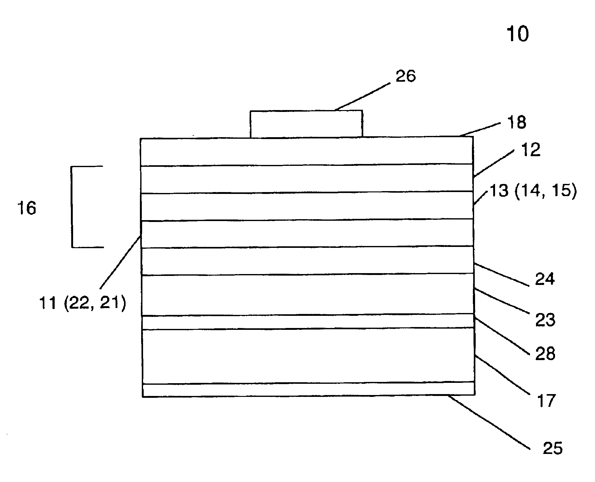
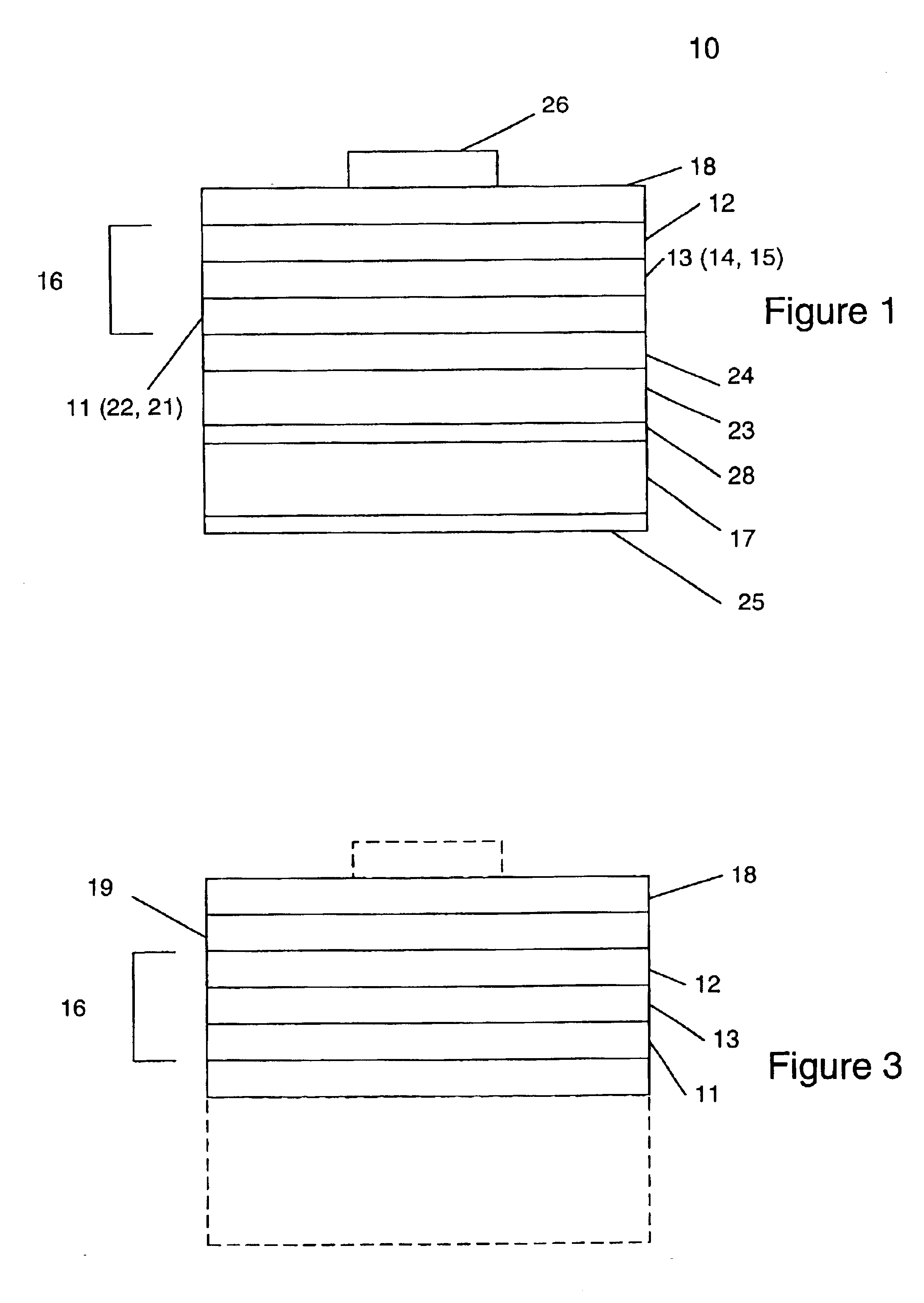
[0043]The present invention is a semiconductor structure for light emitting devices that can emit in the red to ultraviolet portion of the electromagnetic spectrum. In a first embodiment, the structure includes a Group III nitride active portion positioned between a first n-type Group III nitride cladding layer and a second n-type Group III nitride cladding layer. The active portion preferably includes an active layer and a quantum well or a multiple quantum well as described further later herein. The second n-type cladding layer is characterized by the substantial absence of magnesium (i.e., magnesium may be present, but only in amounts that are so small as to have no functional effect on the semiconductor device). The semiconductor structure itself is further characterized by a p-type Group III nitride layer, which is positioned in the semiconductor structure such that the second n-type cladding layer is between the p-type layer and the active layer. In addition, the active layer ...


PUM


Abstract

The present invention is a semiconductor structure for light emitting devices that can emit in the red to ultraviolet portion of the electromagnetic spectrum. The structure includes a first n-type cladding layer of AlxInyGa1−x−yN, where 0≦x≦1 and 0≦y<1 and (x+y)≦1; a second n-type cladding layer of AlxInyGa1−x−yN, where 0≦x≦1 and 0≦y<1 and (x+y)≦1, wherein the second n-type cladding layer is further characterized by the substantial absence of magnesium; an active portion between the first and second cladding layers in the form of a multiple quantum well having a plurality of InxGa1−xN well layers where 0<x<1 separated by a corresponding plurality of AlxInyGa1−x−yN barrier layers where 0≦x≦1 and 0≦y≦1; a p-type layer of a Group III nitride, wherein the second n-type cladding layer is positioned between the p-type layer and the multiple quantum well; and wherein the first and second n-type cladding layers have respective bandgaps that are each larger than the bandgap of the well layers. In preferred embodiments, a Group III nitride superlattice supports the multiple quantum well.

Description

[0001]This is a continuation in part of application Ser. No. 09 / 760,635 filed Jan. 16, 2001 for, “Group III Nitride LED with Undoped Cladding Layer.” This application also claims priority from Provisional Application No. 60 / 294,445 filed May 30, 2001 for, “Multi-Quantum Well Light Emitting Diode Structure.” This application incorporates entirely by reference co-pending and commonly-assigned applications Ser. No. 09 / 706,057 filed Nov. 3, 2000 for “Group III Nitride Light Emitting Devices with Gallium-Free Layers,” and Ser. No. 60 / 298,835 filed Jun. 15, 2001 for “Ultraviolet Light Emitting Diode.”BACKGROUND OF THE INVENTION[0002]The present invention relates to semiconductor structures of light emitting devices, particularly light emitting diodes and laser diodes formed from Group III nitrides, which are capable of emitting light in the red to ultraviolet portions of the electromagnetic spectrum.[0003]Photonic semiconductor devices fall into three categories: devices that convert elec...

Claims


Application Information

Patent Timeline
Patent Type & Authority Patents(United States)
IPC IPC(8): H01L33/00H01L33/02H01L33/06H01L33/14H01L33/32H01S5/343
CPCB82Y20/00H01L33/02H01S5/343H01L33/32H01L33/06H01L33/14H01L33/04
Inventor EDMOND, JOHN ADAMDOVERSPIKE, KATHLEEN MARIEKONG, HUA-SHUANGBERGMANN, MICHAEL JOHNEMERSON, DAVID TODD
Owner CREE INC
Why Eureka
Try Eureka