Method for forming contact holes in a semiconductor device

Active Publication Date: 2016-04-14
SEMICON MFG INT (SHANGHAI) CORP
View PDF4 Cites 1 Cited by
  • Summary
  • Abstract
  • Description
  • Claims
  • Application Information

AI Technical Summary

Benefits of technology

[0006]In embodiments of the present invention, a method of forming contact holes includes forming a sacrificial layer in the contact hole regions and then, after forming an interlayer dielectric layer in the non-contact hole regions, removing the sacrificial layer to expose the contact holes. In contrast, in the conventional method, the interlayer dielectric layer is etched to form contact holes, which can cause damages to the contact hole

Problems solved by technology

In contrast, in the conventional method, the interlayer dielectric layer is etch

Method used


Image

  • Method for forming contact holes in a semiconductor device
  • Method for forming contact holes in a semiconductor device
  • Method for forming contact holes in a semiconductor device

Examples


Example

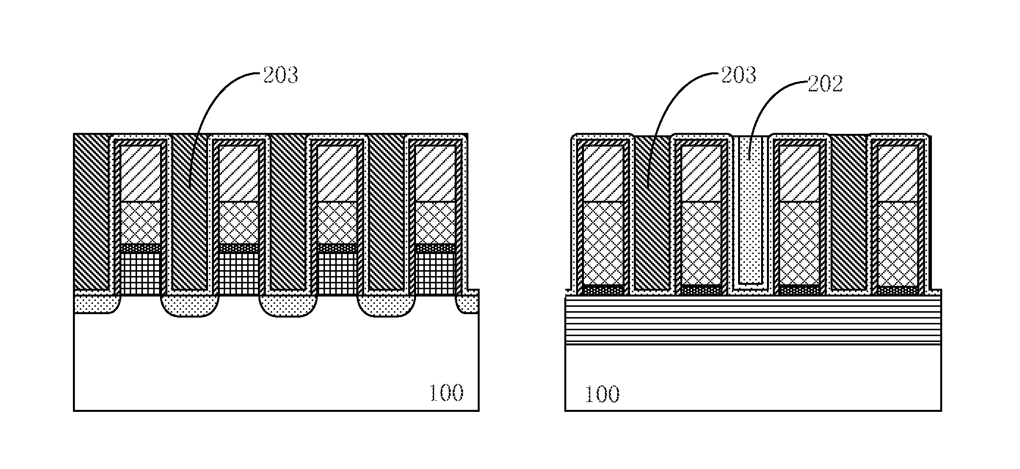
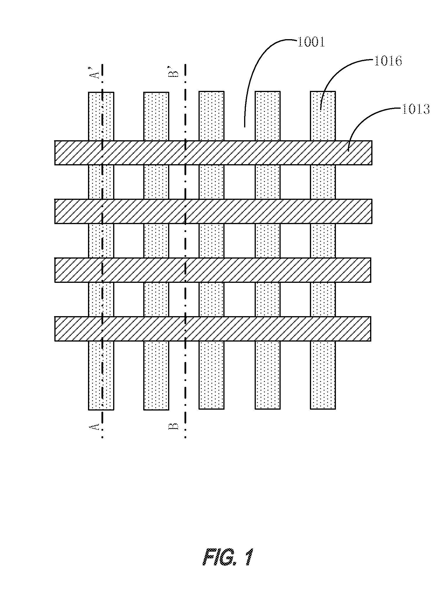
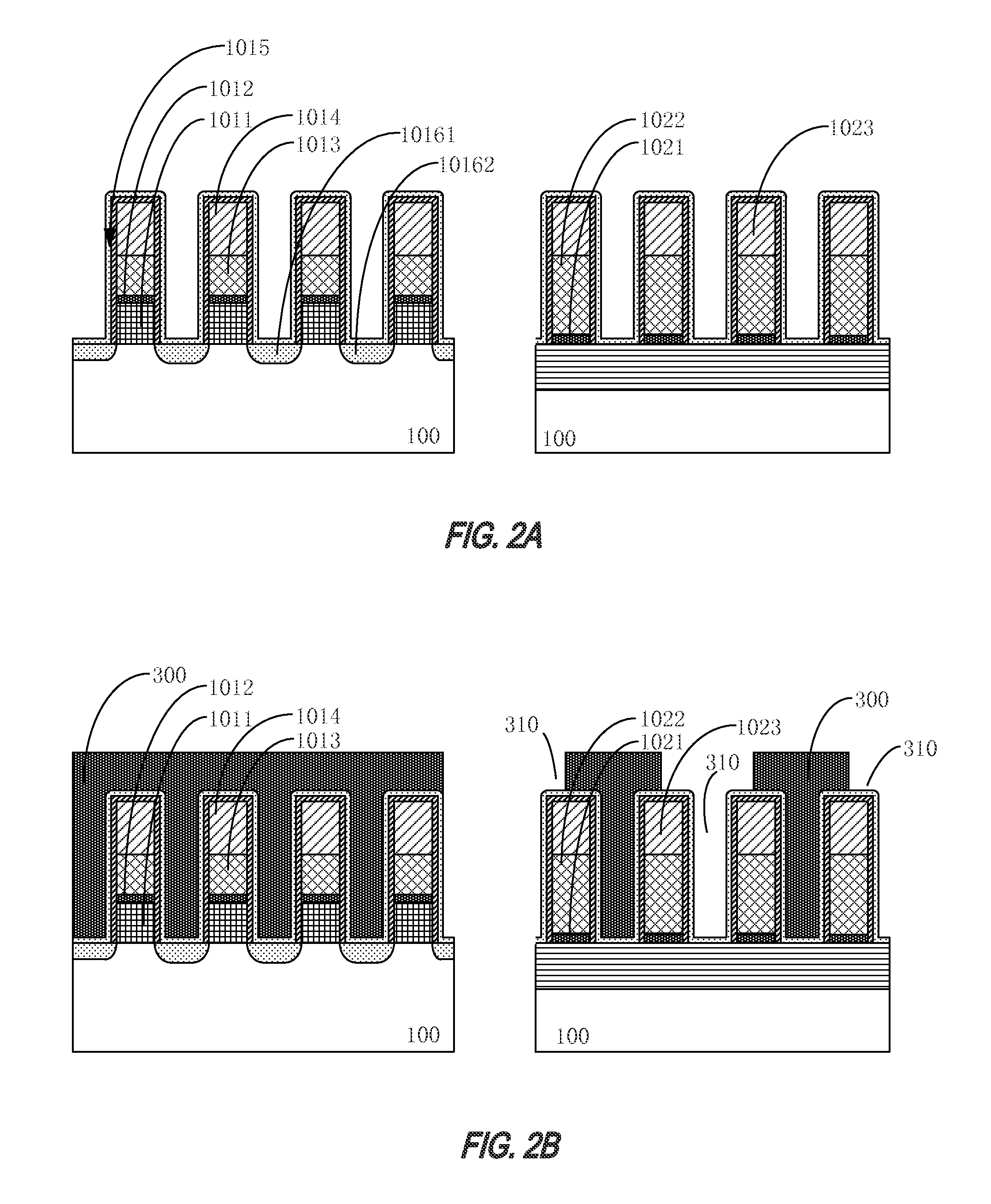
[0021]In the following description, numerous specific details are provided for a thorough understanding of the present invention. However, it should be appreciated by those of skill in the art that the present invention may be realized without one or more of these details. In other examples, features and techniques known in the art will not be described for purposes of brevity.

[0022]It should be understood that the drawings are not drawn to scale, and similar reference numbers are used for representing similar elements. Embodiments of the invention are described herein with reference to cross-section illustrations that are schematic illustrations of idealized embodiments (and intermediate structures) of the invention. The thickness of layers and regions in the drawings may be exaggerated relative to each other for clarity. Additionally, variations from the shapes of the illustrations as a result, for example, of manufacturing techniques and / or tolerances, are to be expected. Thus, e...


PUM


Abstract

A method for forming a semiconductor device includes forming a device structure having a floating gate, control gate, sidewall spacers, and source and drain regions. The device structure includes contact-hole regions and non-contact-hole regions. The method also includes forming a photo resist layer overlying the contact hole regions in the device structure and exposing the non-contact-hole regions, and forming a protective layer overlying the sacrificial layer and the exposed non-contact-hole regions. Next, an interlayer dielectric layer overlying the protective layer, and CMP (chemical mechanical polishing) is used to remove the inter-layer dielectric layer and the protective layer from above the photo resist. The photo resist layer is then removed from the contact-hole regions to expose contact holes.

Description

CROSS-REFERENCES TO RELATED APPLICATIONS[0001]This application claims priority to Chinese patent application No. 201410527831.4, filed on Oct. 9, 2014, the content of which is incorporated herein by reference in its entirety.BACKGROUND OF THE INVENTION[0002]The present invention relates to a semiconductor structure and method of manufacture, and more particularly to a method for forming contact structures.[0003]Increasing demand of high-density low-cost non-volatile memory has driven aggressive scaling of feature sizes for flash memories. For NOR flash memory devices, the main scaling limitation has been the cell height, and the two main factors in the cell height are the drain spacing and the gate length. The drain spacing has only been scaled insignificantly as technology nodes migrate from 90 nm to 65 nm due to the complexity of the minimum spacing (pitch) in patterning one-dimensional array of the contact holes. Gate length scaling remains a challenge for the NOR flash cell due ...

Claims


Application Information

Patent Timeline
IPC IPC(8): H01L21/768H01L21/027H01L23/535H01L21/02H01L29/788H01L29/66H01L21/3105
CPCH01L21/76897H01L29/66825H01L21/0273H01L23/535H01L21/0217H01L21/0206H01L29/788H01L21/31055H01L2924/0002H01L21/76837H10B41/30H01L2924/00
Inventor YANG, YUN
Owner SEMICON MFG INT (SHANGHAI) CORP
Why Eureka
Try Eureka