Power overlay structure having wirebonds and method of manufacturing same

Active Publication Date: 2016-04-14
GENERAL ELECTRIC CO
View PDF3 Cites 11 Cited by
  • Summary
  • Abstract
  • Description
  • Claims
  • Application Information

AI Technical Summary

Benefits of technology

The invention is about a power overlay (POL) structure and a method of manufacturing it. The POL structure includes a power device with a contact pad and a layer of dielectric material on top of the device. There are metal interconnects that extend through the dielectric layer and are connected to the contact pad. The structure also includes copper wirebonds that are connected to the metal interconnects. The technical effect of this invention is to provide a reliable and efficient way to connect power devices to other components on a semiconductor device.

Problems solved by technology

Currently, there is a trend in the industry toward copper wirebonds, which provide lower electrical resistance, which leads to lower losses and higher efficiencies.
However, copper wirebonds do not form reliable electrical connections to the aluminum metallization of the contact pads.
While copper contact pads could be incorporated into the power device at the time of manufacture, incorporating copper into the power device fabrication process is non-trivial and adds significant development cost and time.
Given that a power module may incorporate power devices from multiple manufacturers, forming reliable wirebonds on those power devices is difficult because the various power devices within the given module could include dissimilar metallization materials.
Even where a power device is provided with copper metallization, coupling copper wirebonds to the copper metallization poses difficulties.
Due to these higher energies, the wirebonding process can damage the power device.
Another issue with copper-to-copper wirebonding is the constriction of current as it flows from the contact pads of the power device to the wirebonds.
While providing a number of wirebonds for each contact pad helps in distributing the current flow, the resistance in the interconnect structure still results in inherent losses.

Method used


Image

  • Power overlay structure having wirebonds and method of manufacturing same
  • Power overlay structure having wirebonds and method of manufacturing same
  • Power overlay structure having wirebonds and method of manufacturing same

Examples


Embodiment Construction

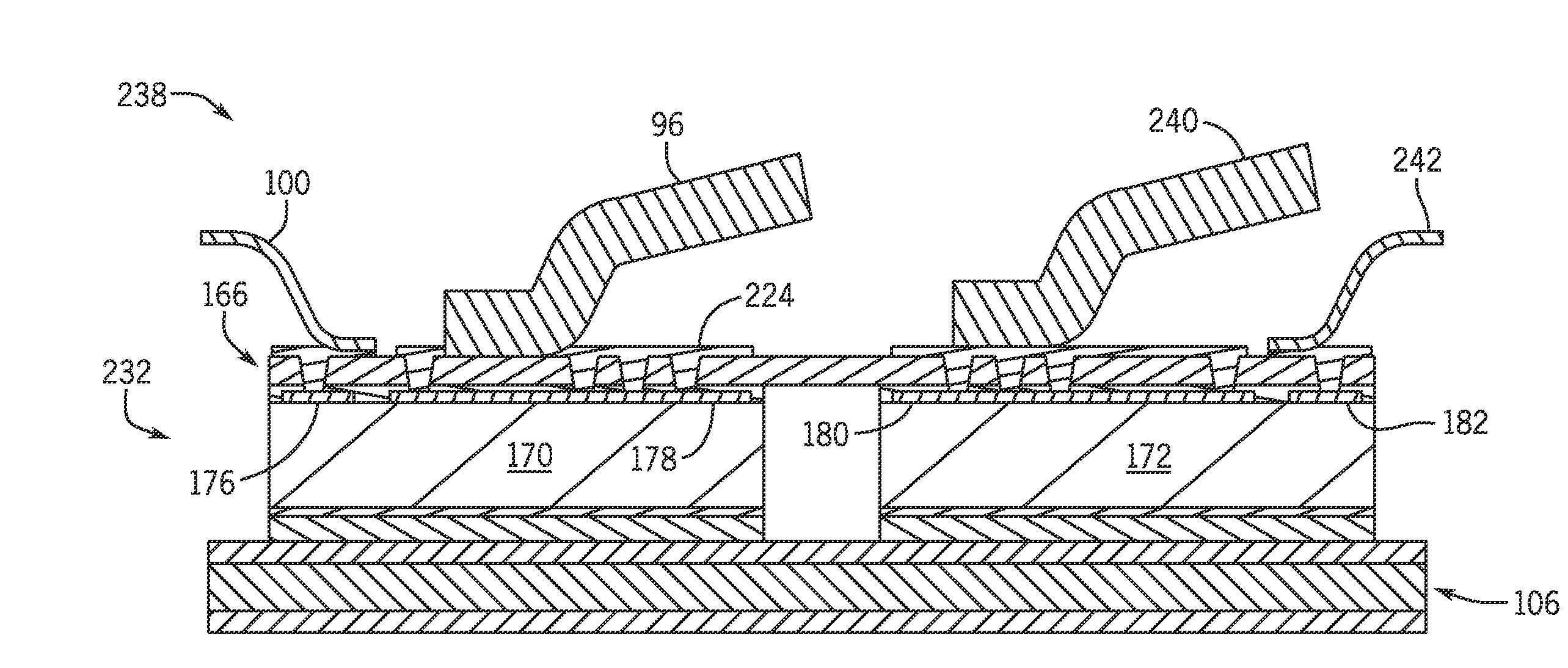
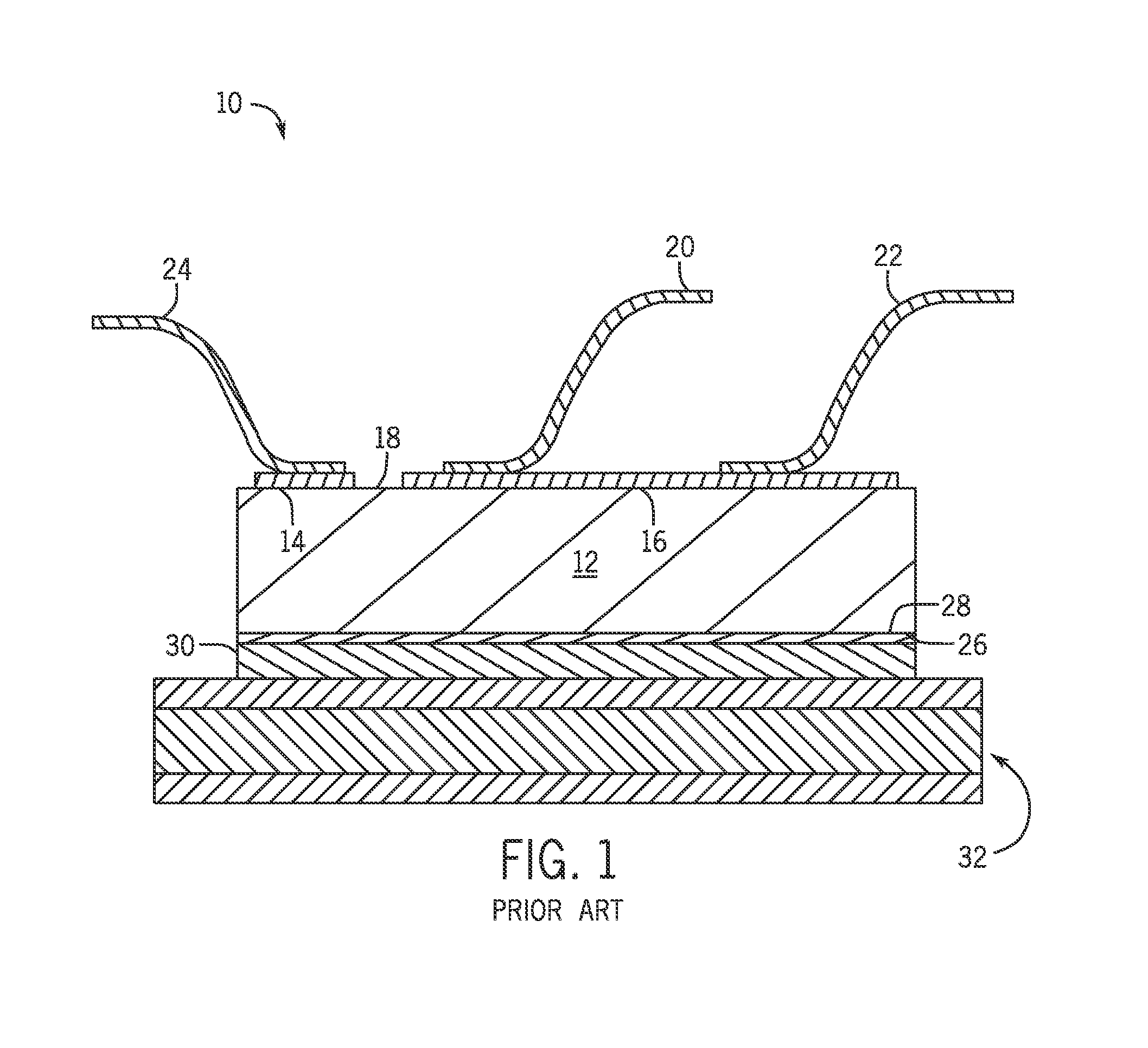
[0026]Embodiments of the present invention provide for a power overlay (POL) structure including a POL interconnect layer, as well as a method of forming such a POL structure. As used herein, the term “POL” describes a structure that enables copper wirebonding of power devices regardless of the material type of the contact pads of the power device. The POL interconnect layer allows for the reliable connection of copper wirebonds to the POL structure regardless of the material of the gate and emitter pads. In addition, the POL interconnect layer is designed to function as a stress buffer that reduces damage to the power device during the process of attaching the wirebonds to the device contact pads. By providing parallel paths for the current to flow through the metallization of the power device before it enters the wirebonds, the POL structure disclosed herein has reduced interconnect resistance and losses as compared to prior art wirebonded power devices.

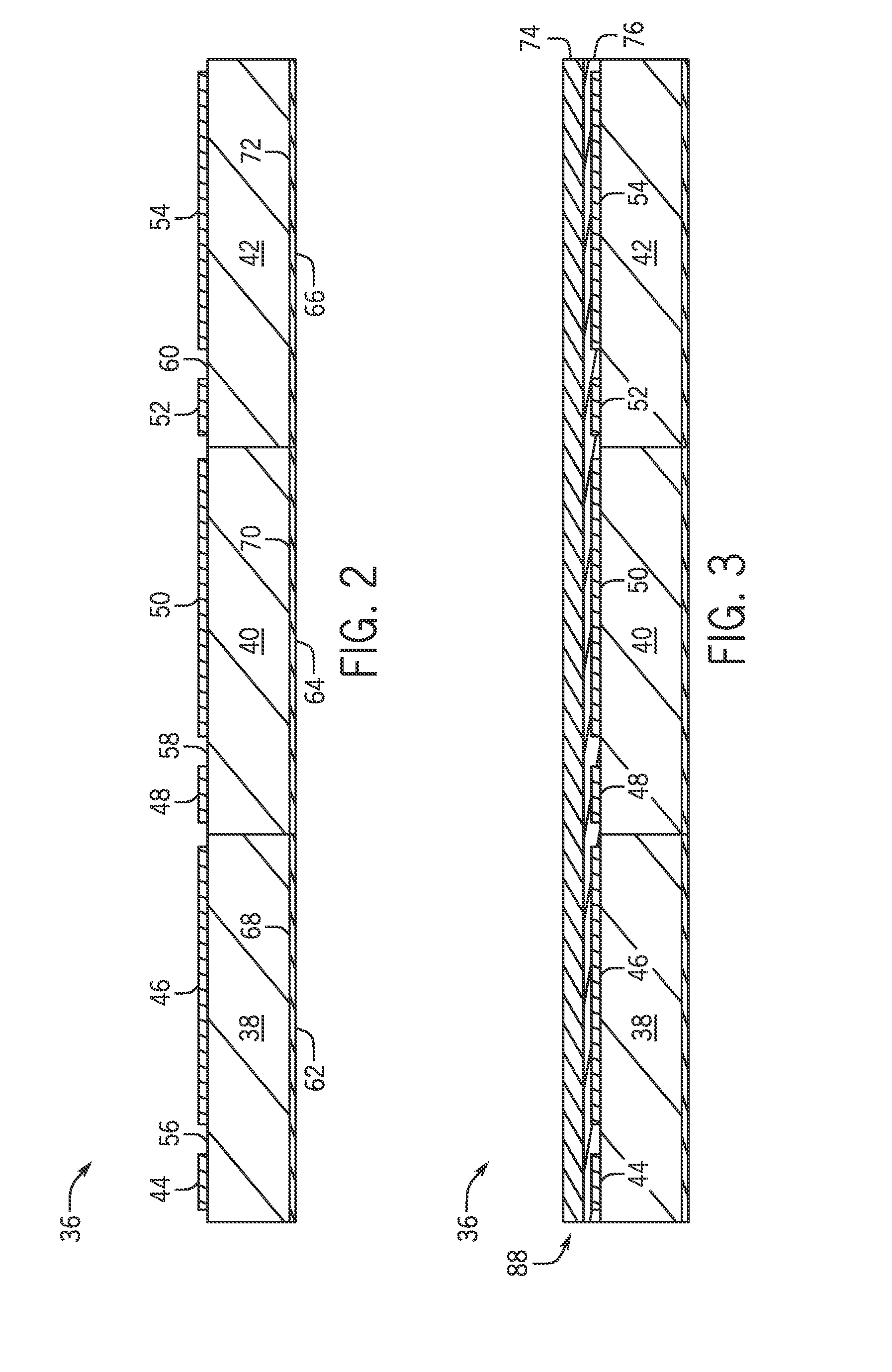
[0027]FIGS. 2-6 depict a te...


PUM


Abstract

A power overlay (POL) structure includes a power device having at least one upper contact pad disposed on an upper surface of the power device, and a POL interconnect layer having a dielectric layer coupled to the upper surface of the power device and a metallization layer having metal interconnects extending through vias formed through the dielectric layer and electrically coupled to the at least one upper contact pad of the power device. The POL structure also includes at least one copper wirebond directly coupled to the metallization layer.

Description

BACKGROUND OF THE INVENTION[0001]Embodiments of the invention relate generally to structures and methods for wirebonding of power devices and, more particularly, to a power overlay (POL) structure that enables copper wirebonding of power devices regardless of the material type of the contact pads of the power device.[0002]Power semiconductor devices are semiconductor devices used as switches or rectifiers in power electronic circuits, such as switched mode power supplies, for example. In use, power semiconductor devices are typically mounted to an external circuit by way of a packaging structure, with the packaging structure providing an electrical connection to the external circuit and also providing a way to remove the heat generated by the devices and protect the devices from the external environment. Power semiconductor devices are provided with a number of input / output (I / O) interconnections to electrically connect the device to an external circuit. These I / O connections may be...

Claims


Application Information

Patent Timeline
IPC IPC(8): H01L23/498H01L21/683H01L21/78H01L25/07H01L21/48
CPCH01L23/49811H01L23/49827H01L23/49838H01L23/49822H01L21/6835H01L21/486H01L21/4853H01L21/78H01L25/072H01L2224/05094H01L2924/13034H01L24/03H01L24/05H01L24/06H01L24/24H01L24/29H01L24/32H01L24/49H01L24/82H01L2224/03466H01L2224/05018H01L2224/05093H01L2224/05624H01L2224/05647H01L2224/0603H01L2224/24137H01L2224/32225H01L2224/45015H01L2224/45147H01L2224/48137H01L2224/4847H01L2224/48847H01L2224/4903H01L2224/4911H01L2224/73265H01L2224/83424H01L2224/83447H01L2924/10253H01L2924/10272H01L2924/10329H01L2924/1033H01L2924/1305H01L2924/13055H01L2924/13091H01L2224/29101H01L2924/13023H01L2224/8203H01L2924/1302H01L2224/04042H01L23/3164H01L23/564H01L23/525H01L23/5283H01L2924/00014H01L24/48H01L2224/05553H01L2224/05554H01L2224/05559H01L2224/49175H01L2224/48138H01L2224/48227H01L2224/4801H01L2224/06181H01L2224/32245H01L2924/014H01L2924/20757H01L2924/20758H01L2924/20759H01L2924/2076H01L2924/00H01L2224/45099H01L2924/207H01L21/76879H01L23/5226H01L23/528H01L24/46H01L24/73H01L24/85H01L25/50H01L2224/05124H01L2224/05147H01L2924/07025H01L2924/1203H01L2924/1301H01L2924/1304
Inventor GOWDA, ARUN VIRUPAKSHAMCCONNELEE, PAUL ALAN
Owner GENERAL ELECTRIC CO
Why Eureka
Try Eureka