Self-compensating gate driving circuit
a self-compensation and gate driving technology, applied in the field of display skill, can solve the problems of affecting the reliability suffering the most serious voltage stress in the entire gate driving circuit, and abnormal image display of the liquid crystal display, so as to promote the reliability of long-term operation and reduce the influence of threshold voltage drift on the operation of the gate driving circui
- Summary
- Abstract
- Description
- Claims
- Application Information
AI Technical Summary
Benefits of technology
Problems solved by technology
Method used
Image
Examples
first embodiment
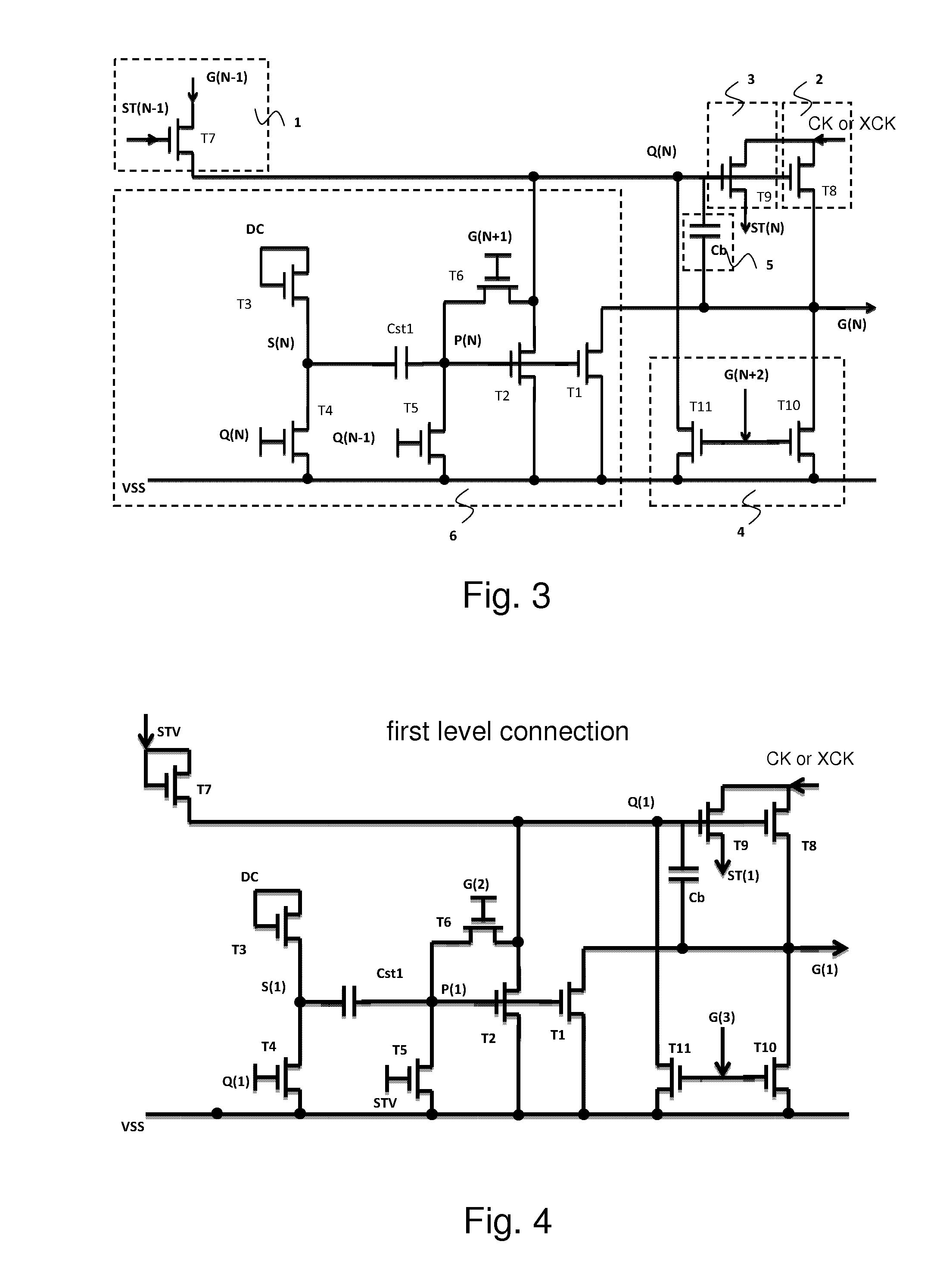
[0045]Please refer to FIG. 6, which is a circuit diagram of the pull-down holding part employed in FIG. 3. The control signal source merely utilizes a DC signal source (DC). The pull-down holding part comprises: a first capacitor Cst1, and an upper electrode plate of the first capacitor Cst1 is electrically coupled to the second circuit point S(N) and a lower electrode plate of the first capacitor Cst1 is electrically coupled to the first circuit point P(N); a first thin film transistor T1, and a gate of the first thin film transistor T1 is electrically coupled to the first circuit point P(N), and a drain is electrically coupled to the Nth horizontal scanning line G(N), and a source is inputted with the DC low voltage VSS; a second thin film transistor T2, and a gate of the second thin film transistor T2 is electrically coupled to the first circuit point P(N), and a drain is electrically coupled to the Nth gate signal point Q(N), and a source is inputted with the DC low voltage VSS;...
second embodiment
[0052]Please refer to FIG. 8 in conjunction with FIG. 6. FIG. 8 is a circuit diagram of the pull-down holding part employed in FIG. 3. In FIG. 8, a second capacitor Cst2 is added on the basis of FIG. 6. An upper electrode plate of the second capacitor Cst2 is electrically coupled to the first circuit point P(N) and a lower electrode plate of the second capacitor Cst2 is inputted with the DC low voltage VSS. The main function of the second capacitor Cst2 is to store the threshold voltage. Certain parasitic capacitance exist in the first thin film transistor T1 and the second thin film transistor T2 themselves and the function of the second capacitor Cst2 can be replaced thereby. Therefore, in actual circuit design, the second capacitor Cst2 can be omitted.
third embodiment
[0053]Please refer to FIG. 9 in conjunction with FIG. 6. FIG. 9 is a circuit diagram of the pull-down holding part employed in FIG. 3. In FIG. 9, a twelfth thin film transistor T12 is added on the basis of FIG. 6. A gate of the twelfth thin film transistor T12 is electrically coupled to the N+1th horizontal scan line G(N+1), and a drain is electrically coupled to the second circuit point S(N), and a source is inputted with the DC low voltage VSS; the main objective of the twelfth thin film transistor T12 is to compensate that voltage level of the Nth gate signal point Q(N) in the first stage is not high enough and leads to a insufficient pulling down of the voltage level to the second circuit point S(N) in the functioning period.
PUM
 Abstract
Description
Claims
Application Information


