Self-compensating gate driving circuit

a self-compensation and gate driving technology, applied in the field of display skill, can solve the problems of affecting the reliability suffering the most serious voltage stress in the entire gate driving circuit, and abnormal image display of the liquid crystal display, so as to promote the reliability of long-term operation and reduce the influence of threshold voltage drift on the operation of the gate driving circui

Active Publication Date: 2017-03-07
TCL CHINA STAR OPTOELECTRONICS TECH CO LTD
View PDF3 Cites 1 Cited by
  • Summary
  • Abstract
  • Description
  • Claims
  • Application Information

AI Technical Summary

Benefits of technology

[0010]An objective of the present invention is to provide a self-compensating gate driving circuit to promote the reliability of the long term operation for the gate driving circuit by a pull-down holding part with self-compensating function. The influence of the threshold voltage drift to the operation of the gate driving circuit is diminished.
[0024]The benefits of the present invention are: the present invention provides a self-compensating gate driving circuit. By utilizing the bootstrap function of the capacitor to control the first circuit point P(N) of the pull-down holding part, it is possible to carry out the function of detecting the threshold voltage of the thin film transistor and to store the threshold voltage at the first circuit point P(N). Accordingly, the variation of the control voltage at the first circuit point P(N) along with the threshold voltage drift of the thin film transistor can be realized. The present invention designs the self-compensating pull-down holding part to promote the reliability of the long term operation for the gate driving circuit and to diminish the influence of the threshold voltage drift to the operation of the gate driving circuit; the pull-down holding part can be designed to be controlled by a set of DC signal source. The design space of the circuit patterns can be saved and the overall power consumption of the circuit can be decreased.

Problems solved by technology

This is a significant factor of influencing the reliability of the gate driving circuit.
However, it is found with actual measurement that the four thin film transistors T6′, T7′, T8′, T9′ still suffer the most serious voltage stress in the entire gate driving circuit even the design of two alternately functioning pull-down holding parts is applied.
Consequently, an abnormal image display of the liquid crystal display will happen.
However, the deactivation leak current of the working thin film transistors will increase when the dimensions of the thin film transistors are increased and the issue cannot be substantially solved.

Method used


Image

  • Self-compensating gate driving circuit
  • Self-compensating gate driving circuit
  • Self-compensating gate driving circuit

Examples


first embodiment

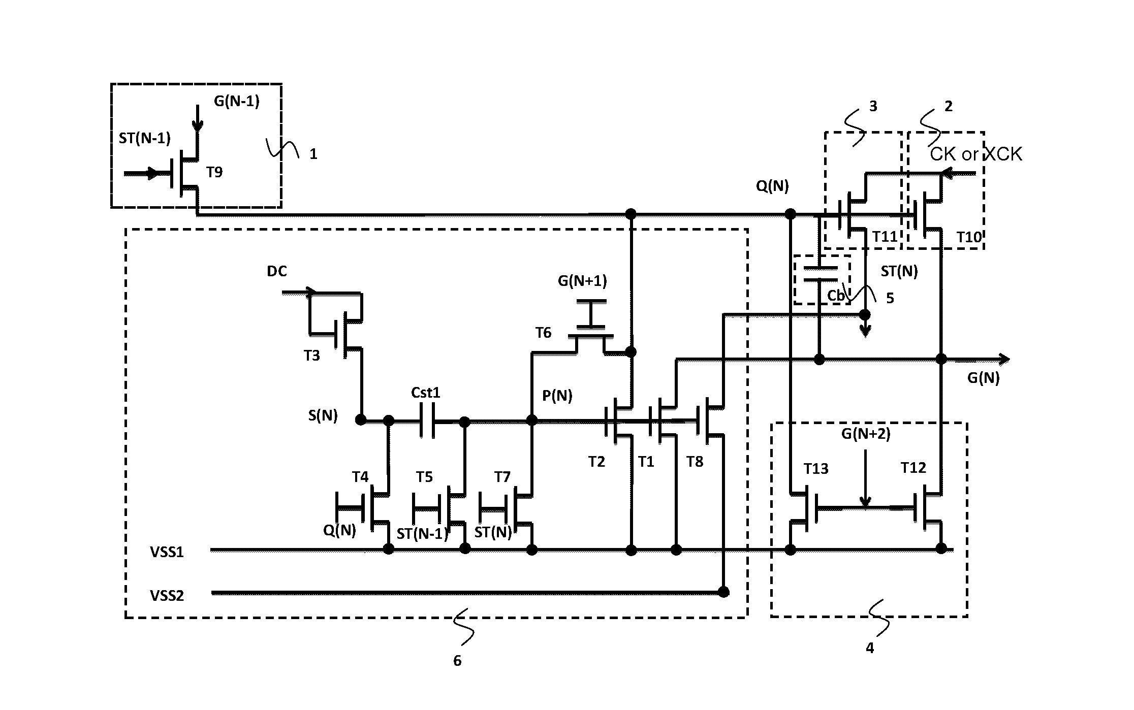
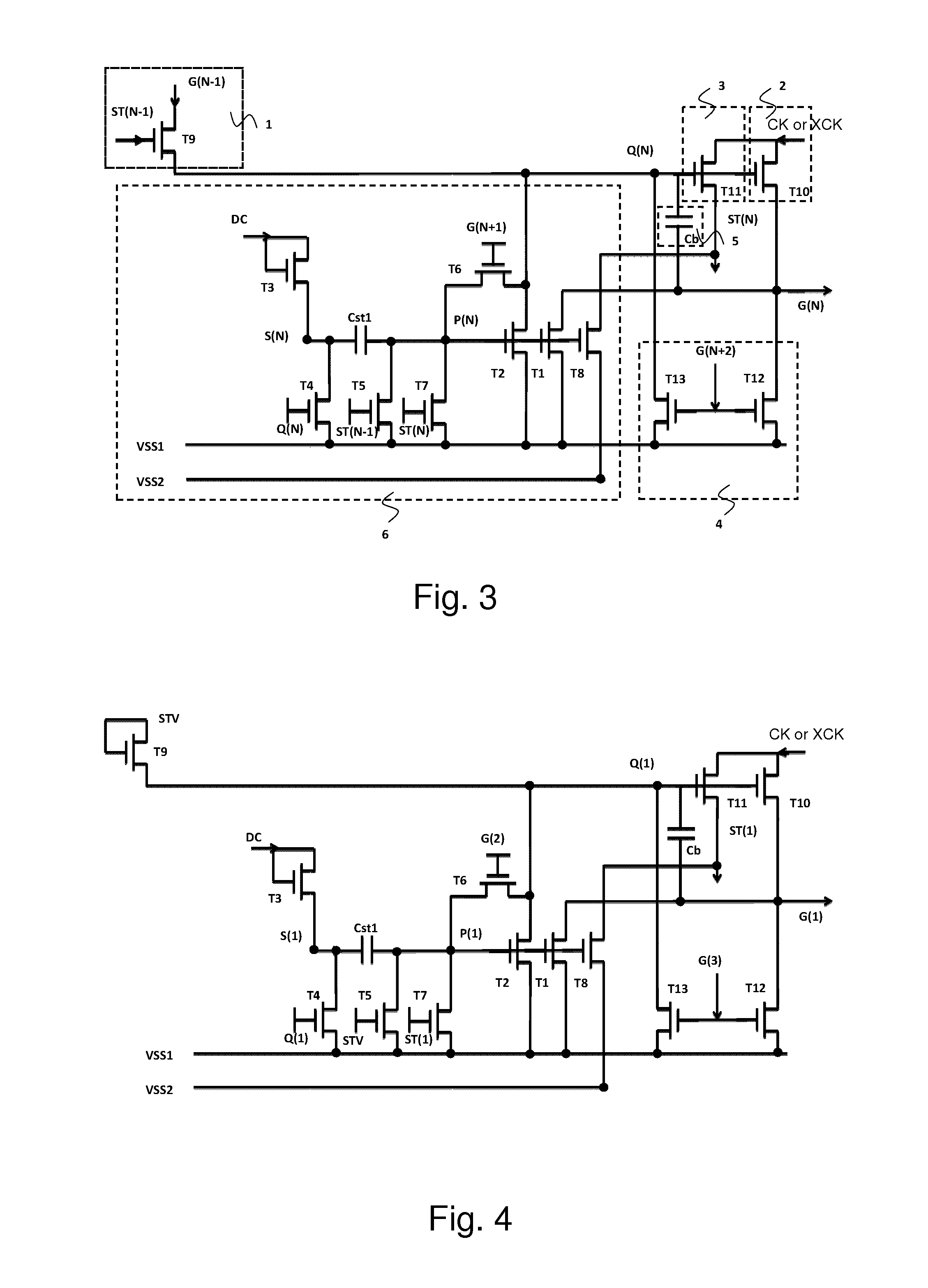
[0047]Please refer to FIG. 6, which is a circuit diagram of the pull-down holding part employed in FIG. 3. The control signal source merely utilizes a DC signal source (DC). The pull-down holding part comprises: a first capacitor Cst1, and an upper electrode plate of the first capacitor Cst1 is electrically coupled to the second circuit point S(N) and a lower electrode plate of the first capacitor Cst1 is electrically coupled to the first circuit point P(N); a first thin film transistor T1, and a gate of the first thin film transistor T1 is electrically coupled to the first circuit point P(N), and a drain is electrically coupled to the Nth horizontal scanning line G(N), and a source is inputted with the first DC low voltage VSS1; a second thin film transistor T2, and a gate of the second thin film transistor T2 is electrically coupled to the first circuit point P(N), and a drain is electrically coupled to the Nth gate signal point Q(N), and a source is inputted with the First DC low...

second embodiment

[0054]Please refer to FIG. 8 in conjunction with FIG. 6. FIG. 8 is a circuit diagram of the pull-down holding part employed in FIG. 3. In FIG. 8, a second capacitor Cst2 is added on the basis of FIG. 6. An upper electrode plate of the second capacitor Cst2 is electrically coupled to the first circuit point P(N) and a lower electrode plate of the second capacitor Cst2 is inputted with the first DC low voltage VSS1. The main function of the second capacitor Cst2 is to store the threshold voltage. Certain parasitic capacitance exist in the first thin film transistor T1 and the second thin film transistor T2 themselves and the function of the second capacitor Cst2 can be replaced thereby. Therefore, in actual circuit design, the second capacitor Cst2 can be omitted.

third embodiment

[0055]Please refer to FIG. 9 in conjunction with FIG. 6. FIG. 9 is a circuit diagram of the pull-down holding part employed in FIG. 3. In FIG. 9, a fourteenth thin film transistor T14 is added on the basis of FIG. 6. A gate of the fourteenth thin film transistor T14 is electrically coupled to the N+1th horizontal scan line G(N+1), and a drain is electrically coupled to the second circuit point S(N), and a source is inputted with the first DC low voltage VSS1; the main objective of the fourteenth thin film transistor T14 is to compensate that voltage level of the Nth gate signal point Q(N) in the first stage is not high enough and leads to a insufficient pulling down of the voltage level to the second circuit point S(N) in the functioning period.


PUM

PropertyMeasurementUnit
voltageaaaaaaaaaa
frequencyaaaaaaaaaa
voltage levelaaaaaaaaaa

Abstract

The present invention provides a self-compensating gate driving circuit, comprising: a plurality of GOA units which are cascade connected, and a Nth GOA unit controls charge to a Nth horizontal scanning line G(n) in a display area, and the Nth GOA unit controls charge to a Nth horizontal scanning line G(n) in a display area, and the Nth GOA unit comprises a pull-up controlling part, a pull-up part, a transmission part, a first pull-down part, a bootstrap capacitor part and a pull-down holding part; the pull-up part, the first pull-down part, the bootstrap capacitor part and the pull-down holding circuit are respectively coupled to a Nth gate signal point Q(N) and the Nth horizontal scanning line G(n), and the pull-up controlling part and the transmission part are respectively coupled to the Nth gate signal point Q(N), and the pull-down holding part is inputted with a first DC low voltage VSS1. The present invention is designed to have the pull-down holding part with self-compensating function to promote the reliability of the long term operation for the gate driving circuit. The influence of the threshold voltage drift to the operation of the gate driving circuit is diminished; the pull-down holding part can be designed to be controlled by a set of DC signal source. The design space of the circuit patterns can be saved and the overall power consumption of the circuit can be decreased.

Description

FIELD OF THE INVENTION[0001]The present invention relates to a display skill field, and more particularly to a self-compensating gate driving circuit.BACKGROUND OF THE INVENTION[0002]GOA (Gate Driver on Array) skill is to integrate the TFT (Thin Film Transistor) of a gate driving circuit on the array substrate and to eliminate the integrated circuit part of the gate driving circuit located outside the array substrate. Accordingly, two aspects of material cost and process is considered to reduce the manufacture cost of the productions. GOA skill is a common gate driving circuit skill used in a present TFT-LCD (Thin Film Transistor-Liquid Crystal Display). The manufacture process is simple and provides great application possibilities. The functions of the GOA circuit mainly comprises: the present gate line outputs a high level signal with charging the capacitor of the shift register unit by using the high level signal outputted from the previous gate line, and then reset is achieved b...

Claims


Application Information

Patent Timeline
Patent Type & Authority Patents(United States)
IPC IPC(8): G09G3/36G02F1/1362
CPCG09G3/3648G02F1/1362G09G3/36G09G2300/04G09G2310/08G09G2330/02G09G3/3677G11C19/184G11C19/28G09G2310/0286G09G2320/043G09G2320/0214G09G2230/00
Inventor DAI, CHAO
Owner TCL CHINA STAR OPTOELECTRONICS TECH CO LTD
Why Eureka
Try Eureka