Integrated multi-terminal devices consisting of carbon nanotube, few-layer graphene nanogaps and few-layer graphene nanoribbons having crystallographically controlled interfaces

a technology of multi-terminal devices and carbon nanotubes, which is applied in the direction of semiconductor devices, electrical equipment, basic electric elements, etc., can solve problems such as limiting the device size reduction

Active Publication Date: 2016-06-02
UNIV OF KENTUCKY RES FOUND
View PDF1 Cites 45 Cited by
  • Summary
  • Abstract
  • Description
  • Claims
  • Application Information

AI Technical Summary

Benefits of technology

[0008]The arrangement and properties of the materials within the device architecture allow for each material of the device architecture to be atomically thin.

Problems solved by technology

This obstacle to device-size reduction is a major impediment to the utilization and control of high-mobility materials such as carbon nanotubes (CNTs) and graphene as device channels for high-frequency applications and in reducing their deleterious excess heat production (Franklin et al.

Method used


Image

  • Integrated multi-terminal devices consisting of carbon nanotube, few-layer graphene nanogaps and few-layer graphene nanoribbons having crystallographically controlled interfaces
  • Integrated multi-terminal devices consisting of carbon nanotube, few-layer graphene nanogaps and few-layer graphene nanoribbons having crystallographically controlled interfaces
  • Integrated multi-terminal devices consisting of carbon nanotube, few-layer graphene nanogaps and few-layer graphene nanoribbons having crystallographically controlled interfaces

Examples


examples

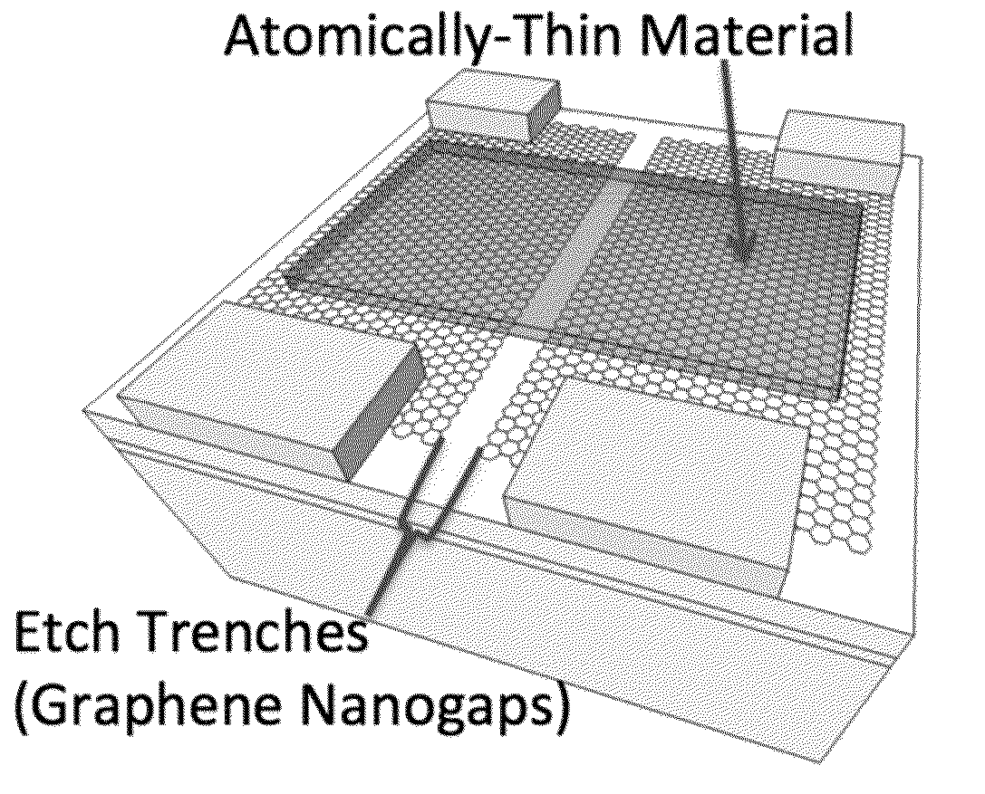
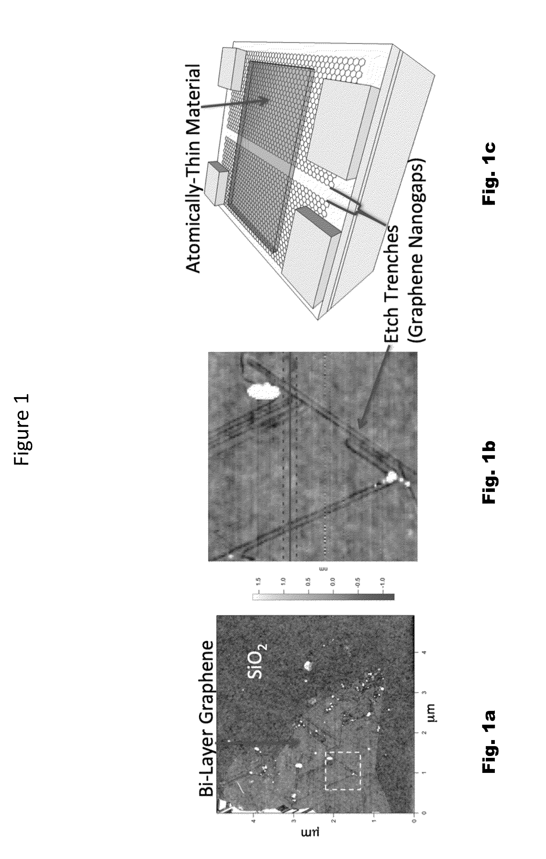
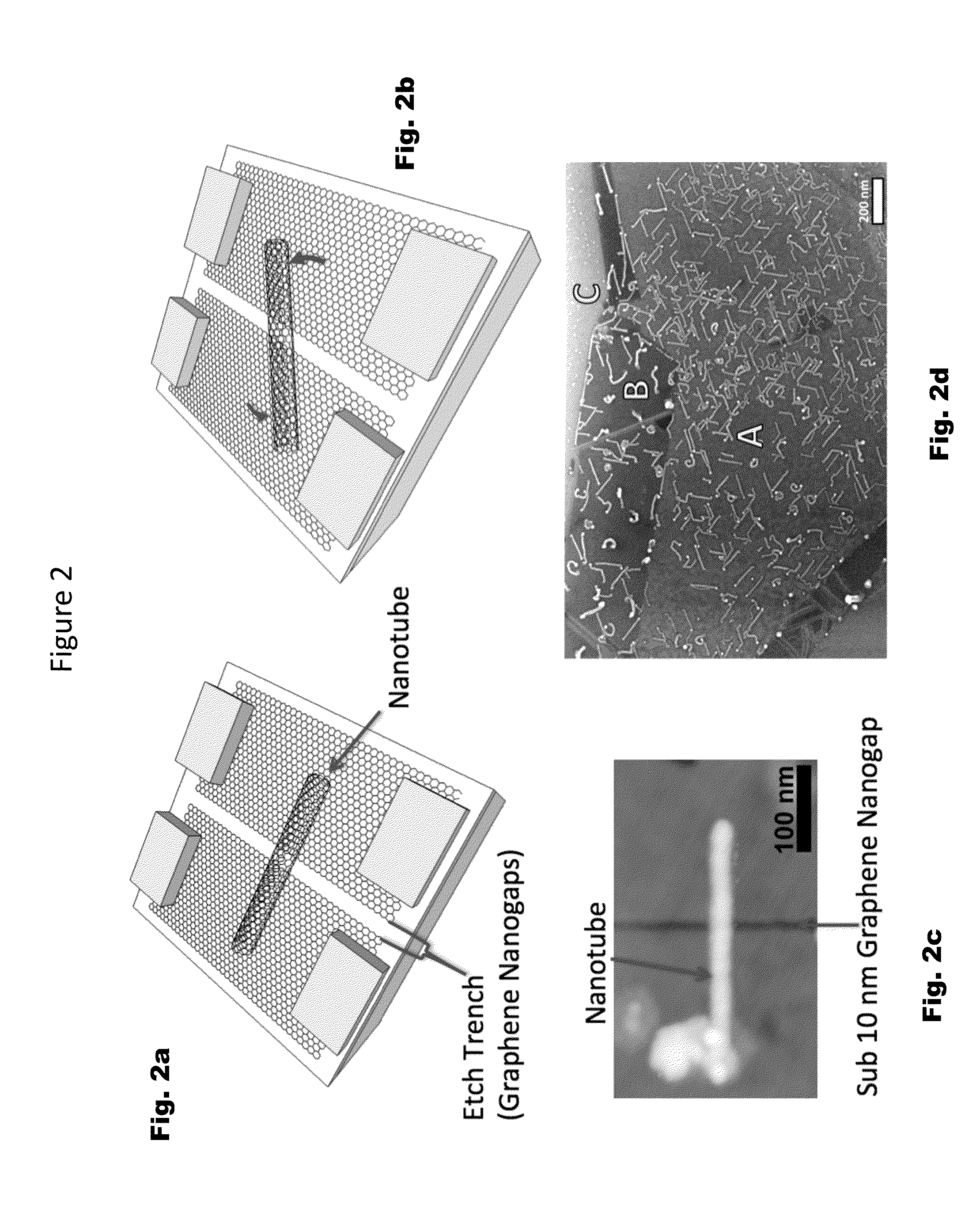
[0045]One of the ultimate goals driving the fields of nanoscience and nanotechnology has been the attainment of atomically precise construction of intricate integrated systems consisting of materials with diverse behavior. Specifically, it is desirable to have high performance conductors, semiconductors, and insulators integrated into complex atomically precise arrangements (Lu et al. Nat. Mater. 6:841 (2007)). The importance of atomic precision in nanoscale synthesis is further supported by the fact that there has been work indicating that the precise crystal orientation and interface quality becomes increasingly important as the individual nanomaterial components are reduced in size (Buldum et al. Phys. Rev. B 63:161403 (2001); Maarouf et al. Phys. Rev. B 83:045402 (2011); Buia et al. Phys. Rev. B 67: 113409 (2003); Hippps et al. Science 294: 536 (2001); Franklin et al. Nano Lett. 12: 758 (2012); Franklin et al. Nat. Nanotechnol. 5: 858 (2010); Xia et al. Nat. Nanotechnol. 6: 179 ...


PUM

PropertyMeasurementUnit
widthaaaaaaaaaa
thickaaaaaaaaaa
widthaaaaaaaaaa

Abstract

The present invention relates to atomically-thin channel materials with crystallographically uniform interfaces to atomically-thin commensurate graphene electrodes and / or nanoribbons separated by nanogaps that allow for nanoelectronics based on quantum transport effects and having significantly improved contact resistances.

Description

RELATED APPLICATIONS[0001]This application claims priority to U.S. Provisional Patent Applications 62 / 084,283, filed Nov. 25, 2014, and 62 / 091,192, filed Dec. 12, 2014, which are hereby incorporated by reference in their entirety.TECHNICAL FIELD[0002]The present invention relates generally to the presence of atomically-thin materials that have a common crystallographically alignment to commensurate nanogap electrodes and nanoribbons. These nanogap electrodes and nanoribbons are unique in that they provide the exact same crystallographic interface to the channel and provide precisely-tuned behaviors and methods of manufacturing such. These controlled electrode interfaces could significantly reduce contact resistances and provide new quantum transport functionality of devices.BACKGROUND[0003]As electrical multi-terminal devices are made smaller, the contacts to the electrodes are critical to their overall performance and are typically ‘weak links’ where significant wasteful deleteriou...

Claims


Application Information

Patent Timeline
Patent Type & Authority Applications(United States)
IPC IPC(8): H01L51/05H01L29/66H01L29/78H01L29/06H01L29/16
CPCH01L51/0558H01L29/0673H01L29/66439H01L29/78H01L29/1606H01L29/42356H01L29/518H01L29/778H01L29/24H01L29/413H01L29/775H01L29/66742H01L29/78681H01L29/78684H01L29/78696H10K85/221H10K10/484
Inventor STRACHAN, DOUGLAS ROBERTHUNLEY, DAVID PATRICK
Owner UNIV OF KENTUCKY RES FOUND
Why Eureka
Try Eureka