
Conductive paste and ceramic electronic component

Active Publication Date: 2016-07-07
MURATA MFG CO LTD
View PDF0 Cites 2 Cited by
  • Summary
  • Abstract
  • Description
  • Claims
  • Application Information

AI Technical Summary

Benefits of technology

The present invention relates to a conductive paste and a ceramic electronic component. The conductive paste has good print characteristics and is easy to apply. The invention uses a Ni powder with fine particles to create fluidity and decrease the viscosity of the paste. The organic solvents used in the invention have different effects on the binder resin component, ensuring that the paste is easy to apply. Using this conductor paste, ceramic electronic components can be made with fewer printing defects. Overall, the invention provides a conductive paste with excellent print characteristics for use in ceramic electronic components.

Problems solved by technology

However, when the conductive paste containing at least the cellulose acetate butyrate resin and an Ni powder is used to form the semiconductor electrode described in PTD 1, a defect may occur upon printing of the conductive paste, in that a printed coating film is not fully formed due to print blurring, for example.
Specifically, the conductive paste as described in PTD 1 containing the cellulose acetate butyrate resin as a main component of the binder may not be transferred to a semiconductor sheet to which the conductive paste should be transferred, leading to a printing defect.
This printing defect is caused by a decrease in the fluidity (increase in the viscosity) of the conductive paste.
It is assumed that this decrease in the fluidity of the conductive paste is due to an insufficient amount of adsorption of the cellulose acetate butyrate resin onto the surface of the Ni powder.

Method used


Image

  • Conductive paste and ceramic electronic component

Examples


example 3

4. Example 3

Preparation of Sample according to Example 3

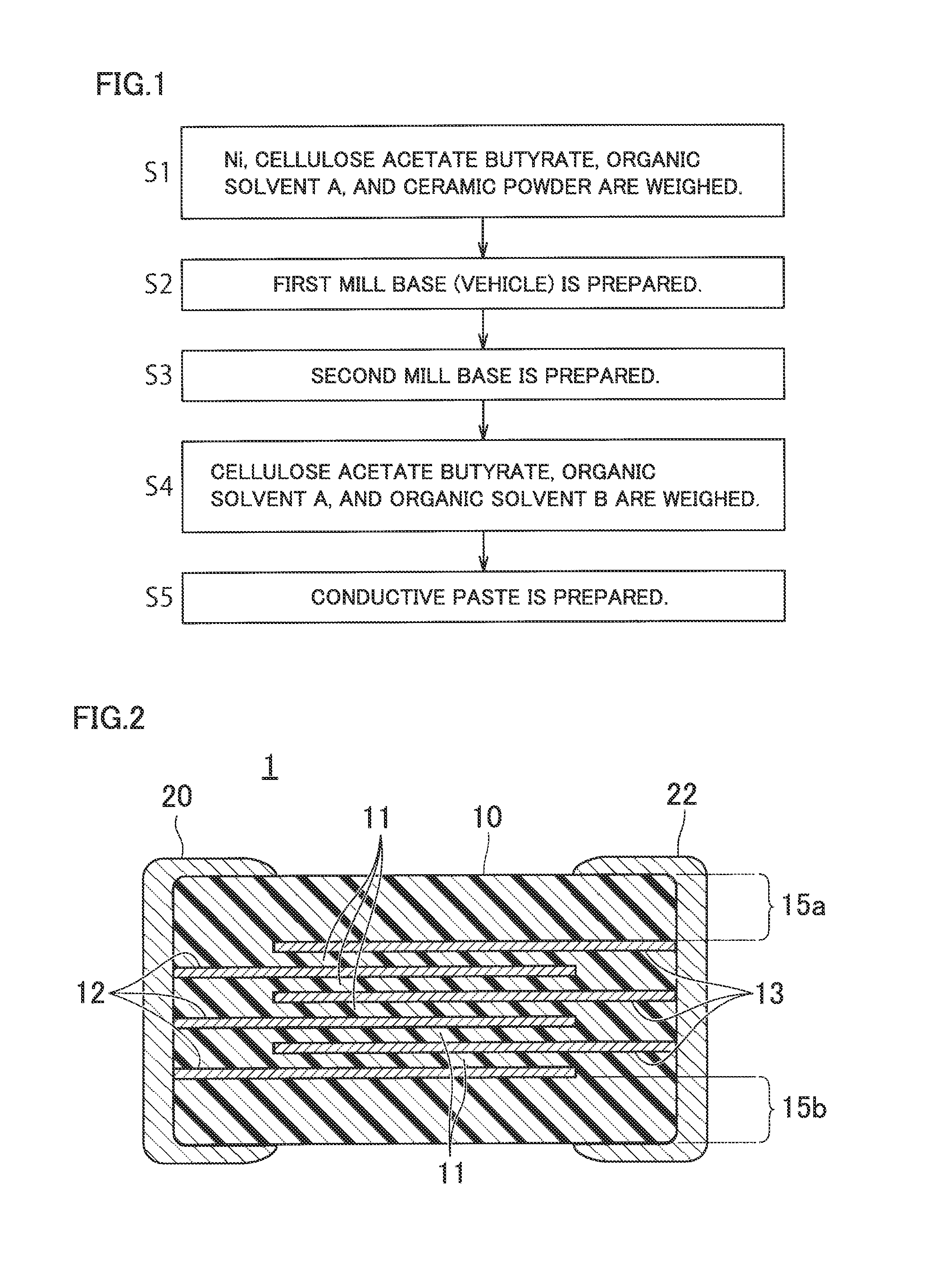
[0096]Conductive pastes as samples 23 to 48 according to Example 3 were prepared by the manufacturing method shown in FIG. 1, using the materials shown in Table 5. The samples according to Example 3 were prepared by setting conditions for organic solvents A and B such that different solvents were selected for each sample.

TABLE 5Example 3MetalOrganic SolventPrimaryBinder ResinRatio ofParticleWeight AverageOrganicCeramicSizeMolecularOrganic Solvent AOrganic Solvent BSolvent BSampleComponentComponent(nm)WeightComponentComponent(wt %)23BaTiO3Ni20027,000AcetophenoneHexane15.024BaTiO3Ni20073,000Anisoleα-Pinene15.025SrTiO3Ni150120,0002-Ethylbutyl AcetateOctane20.026SrTiO3Ni20027,0002-Ethylhexyl AcetateDodecane25.027CaZrO3Ni35032,0002-Hexyl AcetateToluene10.028BaTiO3Ni20015,000n-Propyl AcetateXylene15.029BaTiO3Ni15015,000n-Hexyl AcetateDodecane12.030BaTiO3Ni50140,000Ethyl AcetateMethylcyclohexane30.031BaTiO3Ni40027,000Butyl AcetateD-li...


PUM

PropertyMeasurementUnit
Particle sizeaaaaaaaaaa
Nanoscale particle sizeaaaaaaaaaa
Sizeaaaaaaaaaa

Abstract

A conductive paste obtained by adding an organic solvent B to a vehicle containing a Ni powder, a binder resin component, and an organic solvent A. The Ni powder has an average primary particle size of 30 to 400 nm. The binder resin component is cellulose acetate butyrate. Organic solvent A is a solvent having a Δδ value of 11.5 or less with the cellulose acetate butyrate. Organic solvent B is a solvent having a Δδ value from 11.5 to 25.0 with the cellulose acetate butyrate. A ratio of the organic solvent B relative to a total of the organic solvent A and the organic solvent B is 5.0 to 40.0 wt %.

Description

CROSS REFERENCE TO RELATED APPLICATIONS[0001]The present application is a continuation of International application No. PCT / JP2014 / 066770, filed Jun. 25, 2014, which claims priority to Japanese Patent Application No. 2013-192295, filed Sep. 17, 2013, the entire contents of each of which are incorporated herein by reference.FIELD OF THE INVENTION[0002]The present invention relates to a conductive paste and a ceramic electronic component.BACKGROUND OF THE INVENTION[0003]PTD 1 describes a semiconductor electrode containing at least an Ag powder, an In powder, and a cellulose acetate butyrate resin (binder resin), wherein the Ag powder / In powder in terms of weight ratio is preferably 1 to 4.[0004]PTD 1 also describes a method for manufacturing a semiconductor electrode including the steps of applying a conductive paste containing the above-described components onto a semiconductor, and drying the applied conductive paste by heating to a temperature higher than a melting point of In.[000...

Claims


Application Information

Patent Timeline
IPC IPC(8): C09D5/24
CPCC09D5/24C08L1/14H01G4/30H01B1/22H01G4/0085H01G4/12C08K3/08C08K3/22C08K2003/0862C08K2003/2206C08K2003/2237C08K2003/2244C08K2201/001C08K2201/011B05D5/12
Inventor ISHIKAWA, MASAHITOOGATA, NAOAKI
Owner MURATA MFG CO LTD
Learn More