Touch panel and method for forming a touch structure

a technology of touch panel and structure, applied in the direction of instruments, double resist layers, non-metallic protective coating applications, etc., can solve the problems of complicated conventional process and need additional processes, and achieve the effect of improving the display effect of the touch panel and simplifying manufacturing processes

Active Publication Date: 2016-07-07
TRENDON TOUCH TECHNOLOGY CORPORATION
View PDF12 Cites 2 Cited by
  • Summary
  • Abstract
  • Description
  • Claims
  • Application Information

AI Technical Summary

Benefits of technology

[0007]To solve the issue mentioned above, the present disclosure provides simplified manufacturing processes that also improve the display effect of the touch panel.
[0017]The refractive index of the first anti-etching optical layer and the refractive index of the second anti-etching optical layer can be adjusted, so that the display difference between the etched region and the non-etched region can be reduced. Compared to the conventional process, the present disclosure does not need the steps of removing the hard mask to define the electrode pattern and removing the hard mask to define the trace pattern, so the manufacturing process can be simplified, thereby improving the yield.

Problems solved by technology

Therefore, the conventional process is complicated, and needs additional processes to adjust the display effect of the touch panel.

Method used


Image

  • Touch panel and method for forming a touch structure
  • Touch panel and method for forming a touch structure
  • Touch panel and method for forming a touch structure

Examples


Embodiment Construction

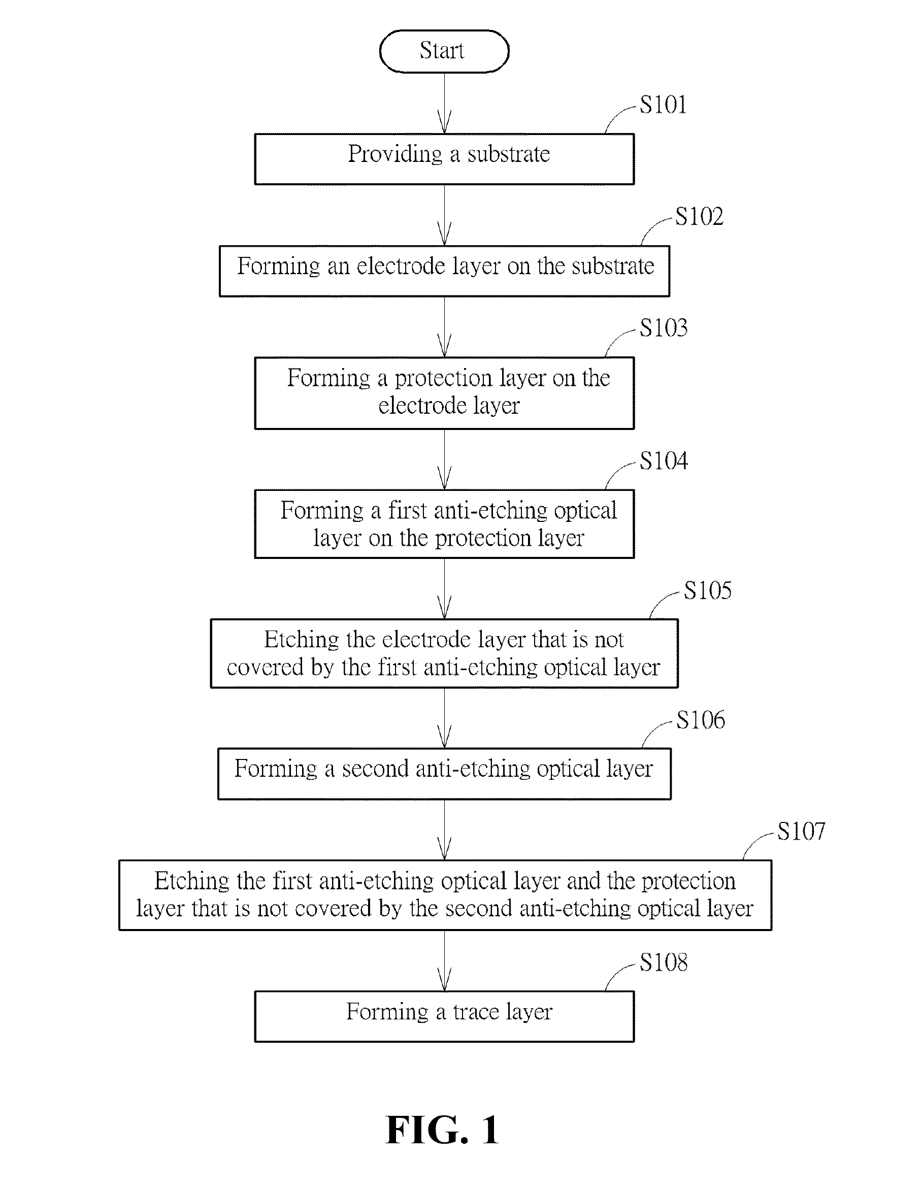
[0039]FIG. 1 is a flow chart showing a manufacturing process of a touch structure according to one or more preferred embodiments of the present disclosure. As shown in FIG. 1, the process comprises the following steps:

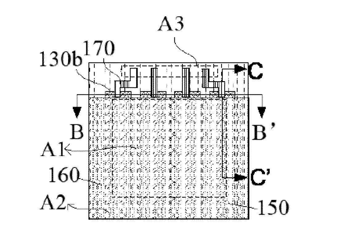
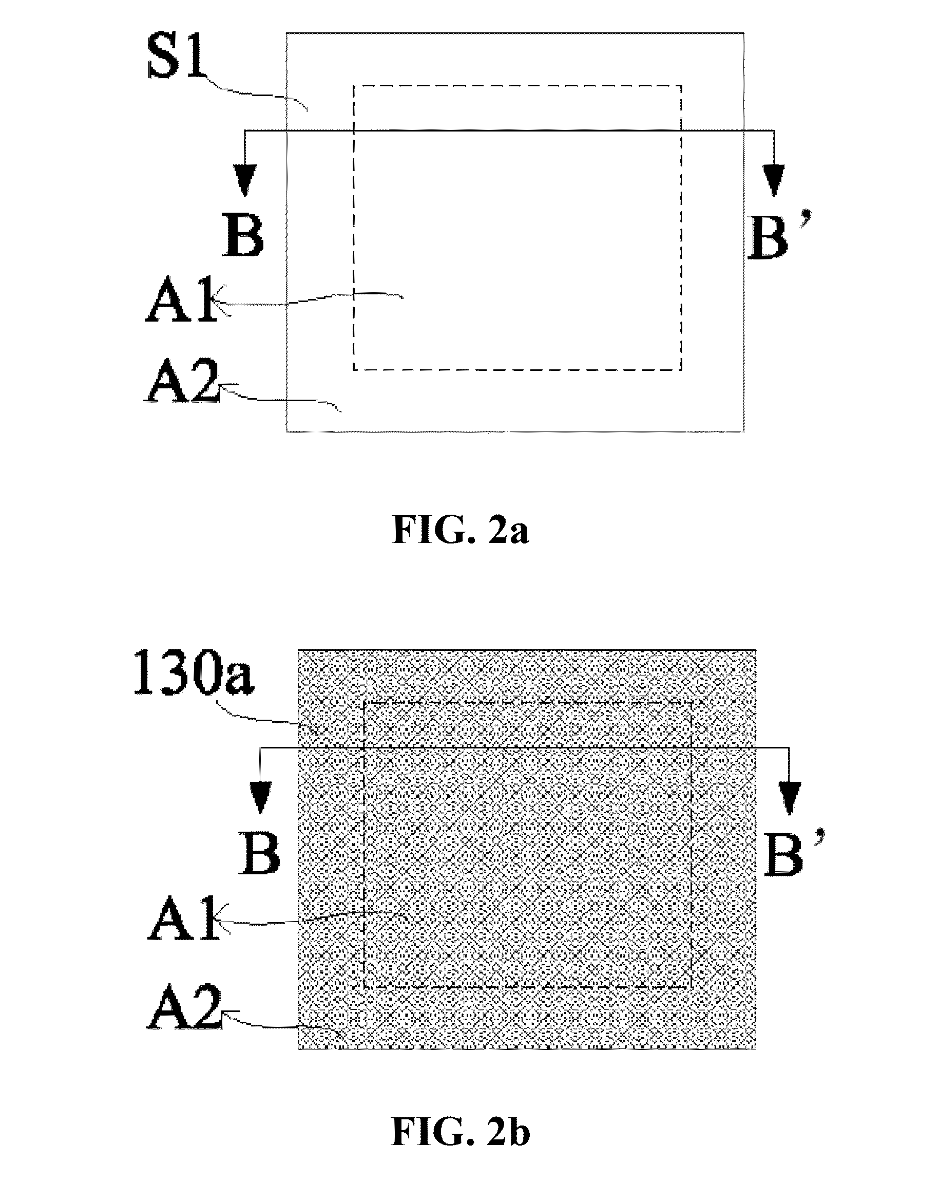
[0040]S101: providing a substrate. Please refer to FIG. 2a and FIG. 2a. In some embodiments, the substrate 110 comprises glass or polyethylene terephthalate (PET). In some embodiments, the substrate 110 has a flat shape or a curved shape so as to be adapted to different types of touch panels. In some embodiments, the substrate 110 is a rigid substrate or a flexible substrate. The substrate 110 has a first surface S1 and an opposite second surface S2. A sensing region A1 (the region delimited by dot lines in FIG. 2a) and a trace, region A2 surrounding the sensing region A1 are defined on the substrate 110.

[0041]S102: forming an electrode layer on the substrate. Please refer to FIG. 2b′ and FIG. 2b. An electrode layer 130a is formed on the first surface S1 of the substra...


PUM


Abstract

A manufacturing process for forming a touch structure at least comprises the following steps. S1: a substrate is provided, a sensing region and a trace region surrounding the sensing region are defined on the substrate; S2: an electrode layer is formed on a substrate; S3: a first anti-etching optical layer is formed on the electrode layer; S4: the electrode layer that is not covered by the first anti-etching optical layer is etched; S5: a second anti-etching optical layer is formed on the first anti-etching optical layer and on the substrate; S6: the first anti-etching optical layer that is not covered by the second anti-etching optical layer is etched; and S7: a trace layer is formed.

Description

BACKGROUND OF THE INVENTION[0001]1. Technical Field[0002]The disclosure relates to the touch sensing technology, and more particularly to touch panel structures and manufacturing processes thereof.[0003]2. Description of the Related Art[0004]In conventional touch electrode manufacturing processes, the main process comprises, forming electrode structures and forming traces, wherein a hard mask is used to define the pattern of the electrode structures and the pattern of the traces, which is removed after the process is performed.[0005]In order to provide a better display effect of a touch panel, an additional optical layer is formed on the touch structure, so as to adjust the display effect of the touch panel.[0006]Therefore, the conventional process is complicated, and needs additional processes to adjust the display effect of the touch panel.SUMMARY OF THE INVENTION[0007]To solve the issue mentioned above, the present disclosure provides simplified manufacturing processes that also ...

Claims


Application Information

Patent Timeline
Patent Type & Authority Applications(United States)
IPC IPC(8): G06F3/041
CPCG06F2203/04103G06F3/0416G06F3/04164G06F3/0443G06F3/0446H05K1/0274H05K1/0289H05K3/28H05K2203/0577
Inventor LIU, CHEN-YULEE, LU-HSING
Owner TRENDON TOUCH TECHNOLOGY CORPORATION
Why Eureka
Try Eureka