Composition for optical film, and films and display device

Active Publication Date: 2016-07-14
SAMSUNG ELECTRONICS CO LTD
View PDF5 Cites 5 Cited by
  • Summary
  • Abstract
  • Description
  • Claims
  • Application Information

AI Technical Summary

Benefits of technology

[0010]An embodiment provides a composition for an optical film capable of simplifying a pro

Problems solved by technology

The visibility and the contrast ratio of the light emitting display device, for example, an organic light emitting display, may be deteriorated by reflection of external light caused by a metal such as an electrode.
However, stacking polymer films results in an optical film of the increased thickness to a thick display device.
In additio

Method used


Image

  • Composition for optical film, and films and display device
  • Composition for optical film, and films and display device
  • Composition for optical film, and films and display device

Examples


preparation example 1

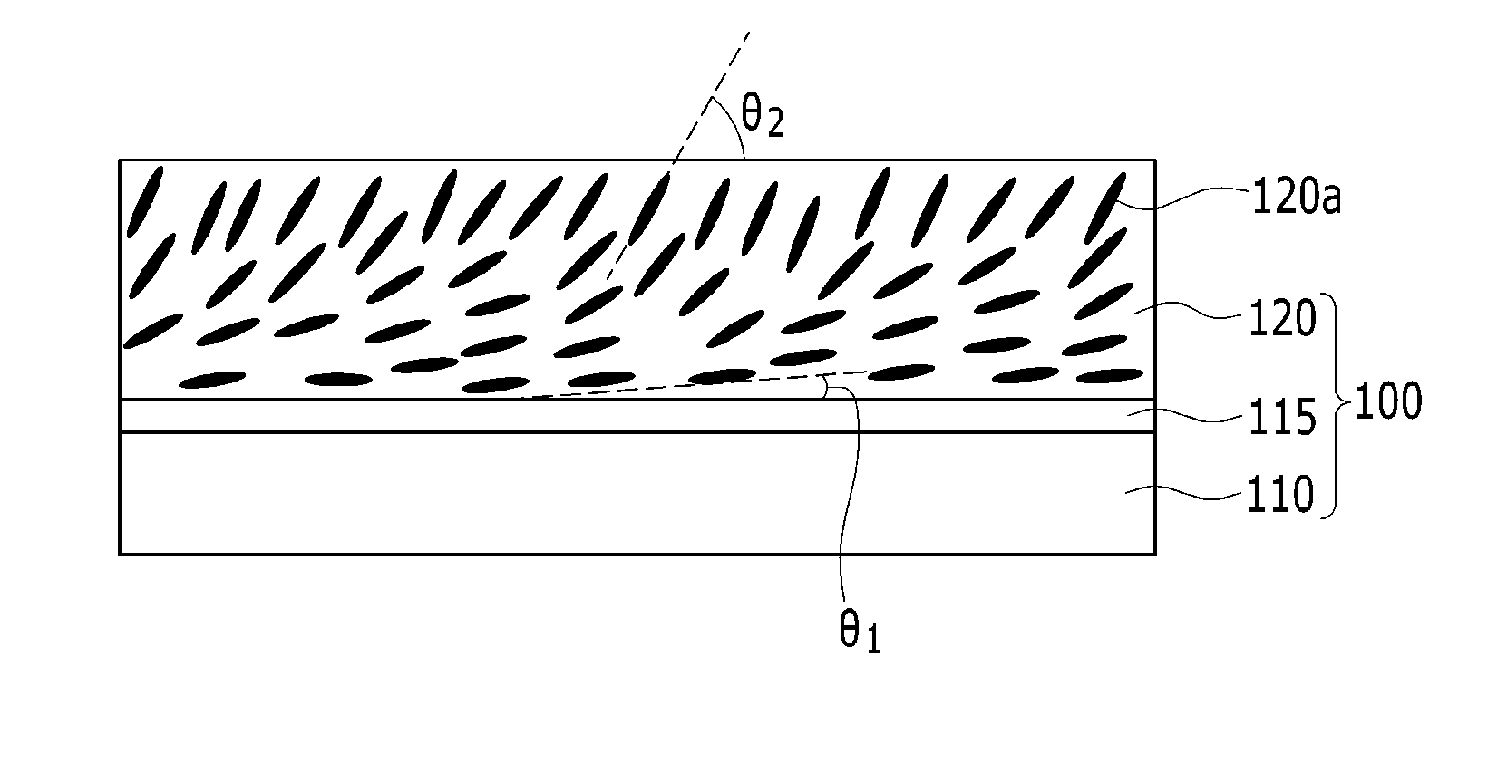
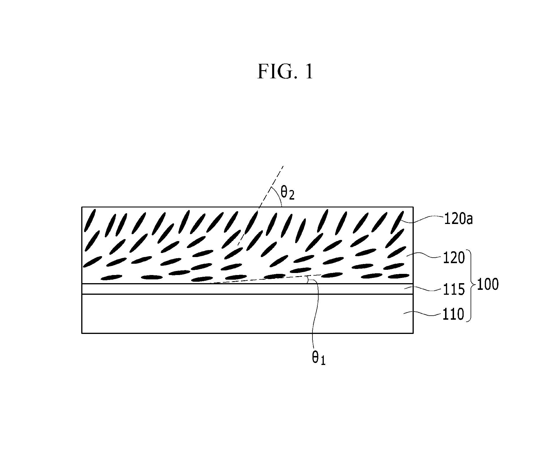
[0283]A composition is prepared by mixing 1 gram (g) of a liquid crystal mixture including a first liquid crystal represented by the following Chemical Formula A-1 (Merck & Co. Ltd.), a second liquid crystal represented by the following Chemical Formula B-1 (Merck & Co. Ltd.), and a third liquid crystal represented by the following Chemical Formula C-1 (Merck & Co. Ltd.), 0.01 g of polysiloxane (MW=12,900) represented by the following Chemical Formula 1aa, 0.03 g of a photoinitiator (Irgacure 907, Ciba Specialty Chemicals Inc.), 0.01 g of a sensitizer (DETX, Sigma-Aldrich Co., Ltd.), and 3.95 g of a mixed solvent of toluene and cyclohexanone (7:3 of wt / wt), and then agitating the mixture on a 45° C. hot plate. Herein, the liquid crystal mixture includes 20.56 wt % of a first liquid crystal, 32.36 wt % of a second liquid crystal, and 47.08 wt % of a third liquid crystal.

preparation example 2

[0284]A composition is prepared by mixing 1 g of the liquid crystal mixture, 0.02 g of polysiloxane represented by the above Chemical Formula 1aa (MW=12,900), 0.03 g of a photoinitiator (Irgacure 907, CIBA Specialty Chemicals Inc.), 0.01 g of a sensitizer (DETX, Sigma-Aldrich Co., Ltd.), and 3.94 g of a mixed solvent of toluene and cyclohexanone (7:3 of wt / wt), and agitating the mixture on a 45° C. hot plate for 1 hour.

preparation example 3

[0285]A composition is prepared by mixing 1 g of the liquid crystal mixture, 0.03 g of polysiloxane represented by the above Chemical Formula 1aa (MW=12,900), 0.03 g of a photoinitiator (Irgacure 907, CIBA Specialty Chemicals Inc.), 0.01 g of a sensitizer (DETX, Sigma-Aldrich Co., Ltd.), and 3.93 g of a mixed solvent of toluene and cyclohexanone (7:3 of wt / wt) and agitating the mixture on a 45° C. hot plate for one hour.


PUM

PropertyMeasurementUnit
Percent by massaaaaaaaaaa
Angleaaaaaaaaaa

Abstract

A composition for an optical film including a liquid crystal and a polysiloxane represented by Chemical Formula 1
wherein in Chemical Formula 1, R1 to R5, L1 to L3, X, Y, Z, T1, T2, a, b, c, and d are the same as described in the detailed description.

Description

CROSS-REFERENCE TO RELATED APPLICATIONS[0001]This application claims priority to and the benefit of Korean Patent Application No. 10-2015-0003679 filed in the Korean Intellectual Property Office on Jan. 9, 2015, the entire contents of which are incorporated herein by reference.BACKGROUND[0002]1. Field[0003]A composition for an optical film, a film, and a display device are disclosed.[0004]2. Description of the Related Art[0005]Commonly used flat panel displays may be classified into a light-emitting display device emitting light by itself and a non-emissive display device requiring a separate light source. An optical film, such as a retardation film, is frequently employed for improving the image quality thereof.[0006]The visibility and the contrast ratio of the light emitting display device, for example, an organic light emitting display, may be deteriorated by reflection of external light caused by a metal such as an electrode. In order to reduce or prevent reflection of the exter...

Claims


Application Information

Patent Timeline
IPC IPC(8): C09K19/56G02B5/30C09K19/52C09K19/20C09K19/30
CPCC09K19/56C09K19/2021C09K19/3068C09K2019/2035G02B5/3016C09K2019/525C09K19/52C09K19/408C09K2019/0448C09K2019/2078C09K2019/3083C09K2219/03C09K2323/03C09K2323/033C08G77/14C08G77/38C08L83/06C08L2203/16B32B2457/20B32B2457/202B32B2457/206C08G77/04C08G77/18C08G77/42C08G77/44C08L83/04C08L83/10G02F1/1335G02F1/133502G02F1/13363G02F1/133633
Inventor LEE, EUN SUNGPARK, SANG HOKAMADA, KOHOHYAMA, TSUYOSHICHUN, SEUNGBUM
Owner SAMSUNG ELECTRONICS CO LTD
Why Eureka
Try Eureka