Compensation film and optical film and display device

Active Publication Date: 2015-05-14
SAMSUNG ELECTRONICS CO LTD
View PDF10 Cites 8 Cited by
  • Summary
  • Abstract
  • Description
  • Claims
  • Application Information

AI Technical Summary

Benefits of technology

The patent describes a compensation film that improves the display quality of a device by reducing the impact of viewing angle and wavelength. This means that the film can produce better results when showing different objects or colors, which can be useful in a range of applications.

Problems solved by technology

In the case of the light emitting display device, for example, an organic light emitting diode (“OLED”) display, the visibility and the contrast ratio may be deteriorated by reflection of the exterior light caused by a metal such as an electrode.
However, a conventional compensation film is strongly dependent upon the wavelength to the incident light, so such a compensation film may effectively operate for light having a certain wavelength, but the effect thereof may be deteriorated for other wavelengths.
In addition, a conventional compensation film may have strong viewing angle dependency.

Method used


Image

  • Compensation film and optical film and display device
  • Compensation film and optical film and display device
  • Compensation film and optical film and display device

Examples


preparation example 1

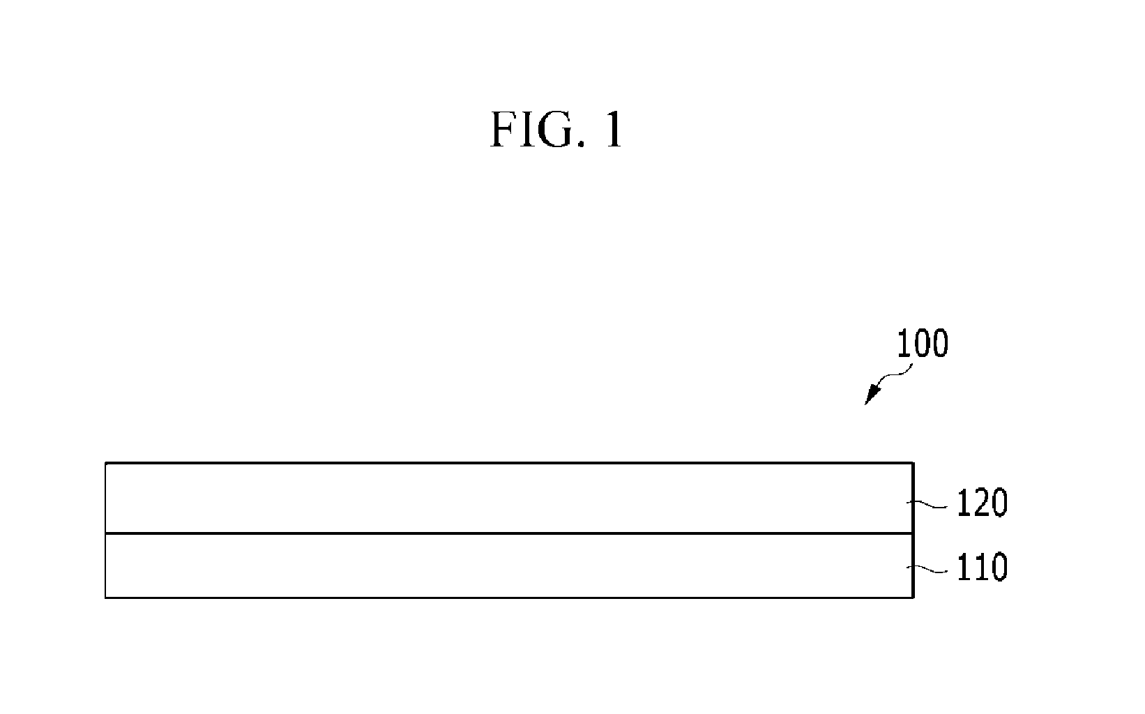
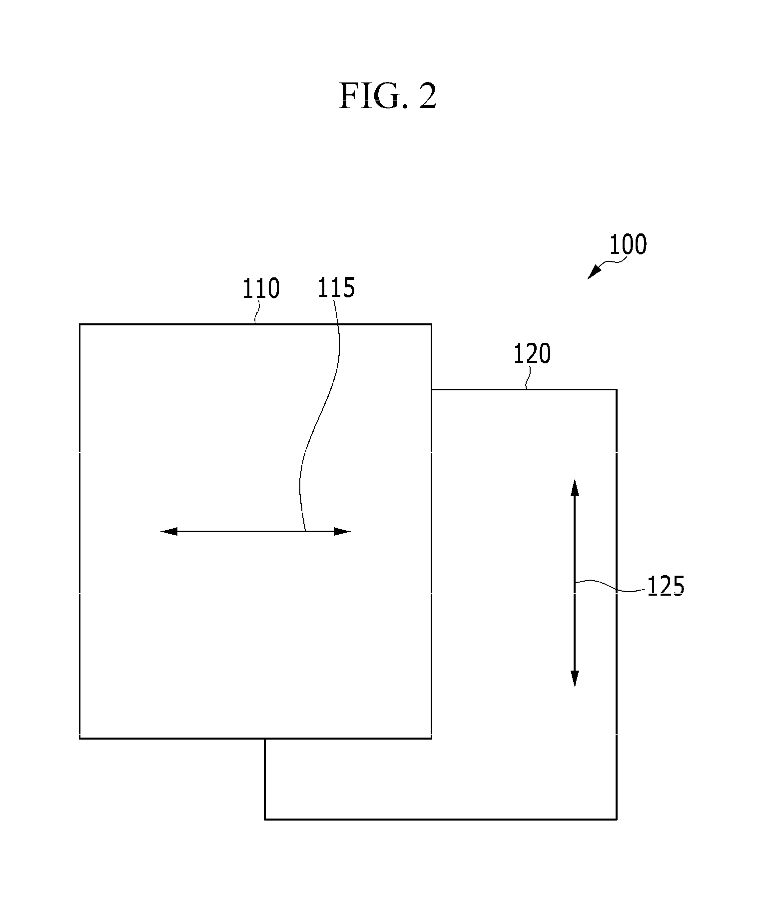
[0115](1) Preparation of First Retardation Layer (A)

[0116]A poly(styrene-co-methacrylic acid) film (T080, manufactured by TOYO STYRENE) having a thickness of 100 μm is elongated in one axial direction (using a tension tester manufactured by Instron) at about 128° C. at a ratio of 50%to 200% to provide a first retardation layer (A) having optical properties shown in the following Table 1.

[0117](2) Preparation of Second Retardation Layer (B)

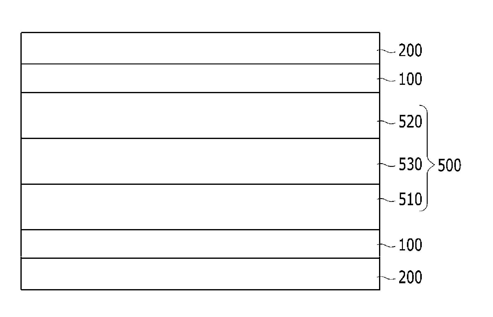
[0118]A 60 μm-thick Z-TAC film (from Fuji Film) is rubbed in one direction and coated with +A plate liquid crystal (RMS03-013C, Merck & Co., Inc.) in a thickness of about 5 μm to about 10 μm and dried in a drying oven at 60° C. for one minute to remove a coating solvent. Subsequently, ultraviolet (“UV”) rays are irradiated thereto at 80 milliwatts per square centimeter (mW / cm2) for 30 seconds in a nitrogen-charged container, so that the liquid crystal molecules are is photo-cross-linked to provide a second retardation layer (B) having the optical p...

preparation example 2

[0121]A compensation film is manufactured in accordance with the same procedure as in Preparation Example 1, except that the first retardation layer (A) and the second retardation layer (B) have the optical properties shown in the following Table 2.

TABLE 2In-plane retardation (Re)ReReReWavelength dispersion(450(550(650Re (450 nm) / Re (650 nm) / nm)nm)nm)Re (550 nm)Re (550 nm)NzA110010309931.0680.964−0.03B10008908481.1230.9531.02* Nz = (Rth / Re) + 0.5

preparation example 3

[0122]A compensation film is manufactured in accordance with the same procedure as in Preparation Example 1, except that the first retardation layer (A) and the second retardation layer (B) have the optical properties shown in the following Table 3.

TABLE 3In-plane retardation (Re)ReReReWavelength dispersion(450(550(650Re (450 nm) / Re (650 nm) / nm)nm)nm)Re (550 nm)Re (550 nm)NzA8387857571.0680.964−0.04B7296406101.1230.9531.01* Nz = (Rth / Re) + 0.5


PUM


Abstract

A compensation film includes a first retardation layer including a polymer having negative birefringence, and a second retardation layer including a liquid crystal having positive birefringence, where the first retardation layer has an in-plane retardation (Re1) of 320 nm to 1050 nm for incident light having wavelength of 550 nm, the second retardation layer has an in-plane retardation (Re2) of 180 nm to 910 nm for the incident light, an entire in-plane retardation (Re0) of the first and second retardation layers for the incident light is a difference between the in-plane retardations of the first and second retardation layers, an angle between slow axes of the first and second retardation layers is 85 to 95 degrees, and the entire in-plane retardation (Re0) of the first and second retardation layers for the wavelength of 450 nm, 550 nm and 650 nm satisfies Re0 (450 nm)<Re0 (550 nm)<Re0 (650 nm).

Description

[0001]This application claims priority to Korean Patent Application No. 10-2013-0137146 filed on Nov. 12, 2013, and all the benefits accruing therefrom under 35 U.S.C. §119, the contents of which are incorporated by reference herein in its entirety.BACKGROUND[0002]1. Field[0003]Embodiments of the invention relate to a compensation film, an optical film, and a display device including the compensation film or the optical film.[0004]2. Description of the Related Art[0005]A flat panel displays may be classified into a light-emitting display device that emits light by itself and a non-emissive display device that includes a separate light source, and a compensation film such as a retardation film is generally employed for improving the image quality thereof.[0006]In the case of the light emitting display device, for example, an organic light emitting diode (“OLED”) display, the visibility and the contrast ratio may be deteriorated by reflection of the exterior light caused by a metal su...

Claims


Application Information

Patent Timeline
IPC IPC(8): G02F1/13363G02B5/30G02F1/1335
CPCG02F1/13363G02F2001/133633G02B5/3083G02F1/133528G02B5/3016G02F2202/40C09K2323/035C09K2323/03G02F1/133633G02B5/30G02F1/1335H10K50/00B32B2457/206B32B2457/202G02F1/133634C09K19/02G02F1/133637
Inventor KIM, HYUNG JUNGAM, SANG AHJUNG, MYUNG SUPCHOI, HYUN-SEOK
Owner SAMSUNG ELECTRONICS CO LTD
Why Eureka
Try Eureka