

Liquid crystal electro-optic device
- Summary
- Abstract
- Description
- Claims
- Application Information
AI Technical Summary
Benefits of technology
Problems solved by technology
Method used
Image

Examples
first preferred embodiment
(First Preferred Embodiment)
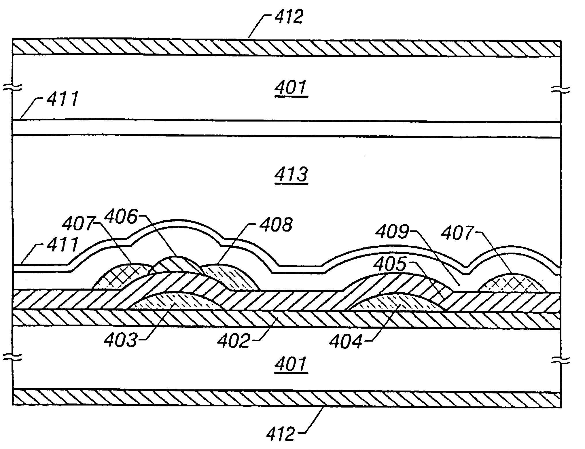
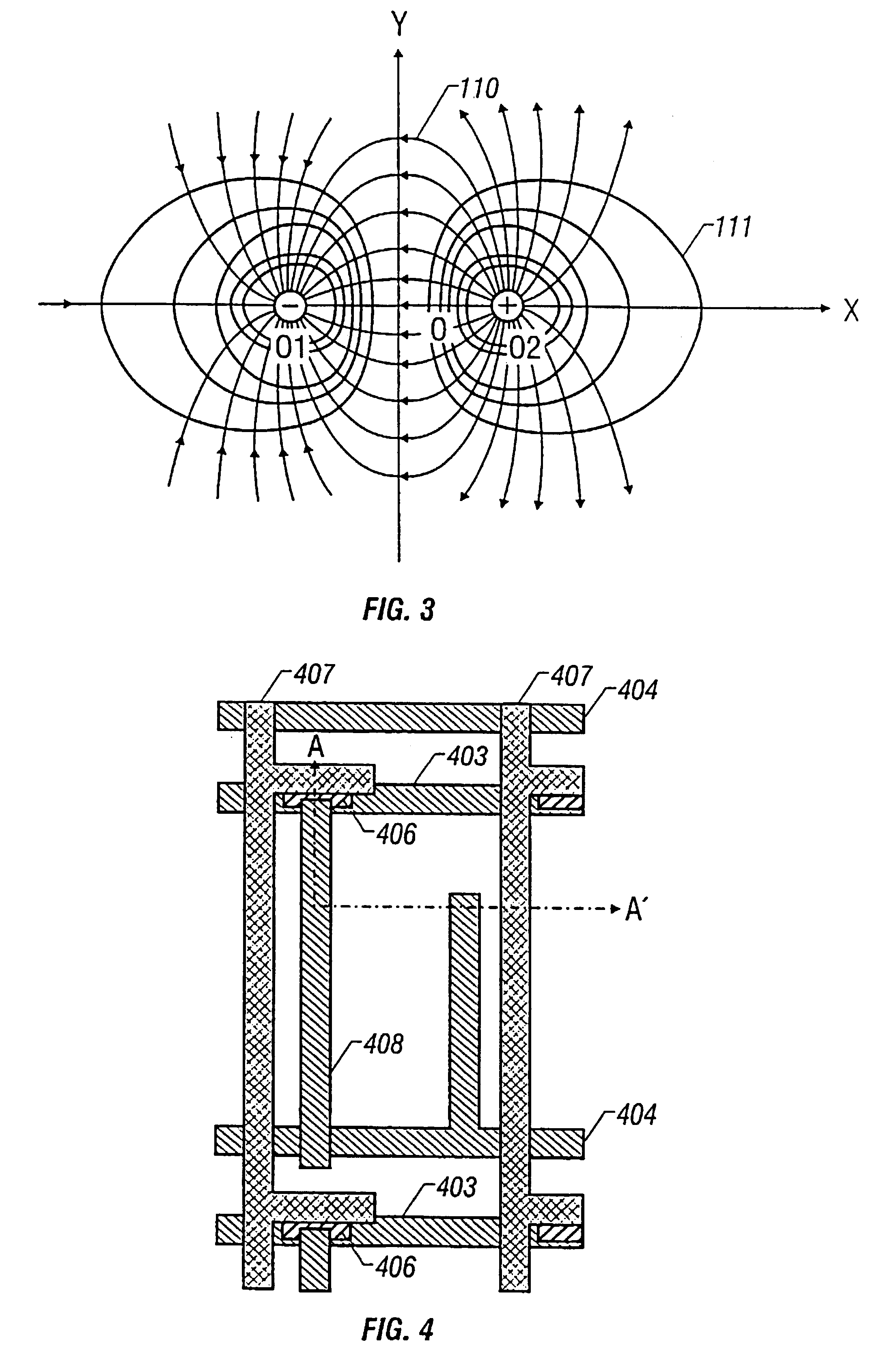
[0082]A silicon oxide film of thickness 1000 to 3000 Å was formed as a base oxide film (402) on a Corning #7059 insulating substrate (401). As the method of forming this silicon oxide film, sputtering in an oxygen atmosphere or plasma CVD can be used. A film of Cr was then formed on this to a thickness of 1000 to 5000 Å and patterned. After that, isotropic plasma etching was carried out using resist as a mask. At this time, the discharge gas voltage was suitably set to give the electrodes curved surfaces. In this way, a gate electrode (403) and a common electrode (404) were formed.
[0083]A gate insulating film (405) consisting of silicon dioxide (SiO2) was then formed so as to cover these electrodes. This film may alternatively consist of silicon nitride (SiN). An amorphous silicon film (406) was then formed on the gate insulating film above the gate electrode. Then, a source electrode (407) and a drain electrode (408) consisting of Al were formed so as to...
second preferred embodiment
(Second Preferred Embodiment)
[0090]The liquid crystal electro-optic device of this preferred embodiment is a monolithic active matrix circuit wherein a peripheral driving circuit is also formed on the substrate. A process for making the device will be described using FIG. 6 and FIGS. 7(A) to 7(E). FIG. 6 is a schematic plan view of a pixel of this preferred embodiment. FIGS. 7(A) to 7(E) are sectional views on the line B-B′B″ in FIG. 6, a process for manufacturing TFTs of a driving circuit being shown on the left side and a process for manufacturing a TFT of an active matrix circuit being shown on the right side. These processes are low temperature polysilicon processes.
[0091]First, a base silicon oxide film (402) was formed on a Corning #1737 first insulating substrate (601). This silicon oxide film may be formed by the same method as that shown in the first preferred embodiment.
[0092]After that, an amorphous silicon film was formed to 300 to 1500 Å, and preferably 500 to 1000 Å, b...
PUM
 Abstract
Description
Claims
Application Information