Organic light emitting display panel and method of manufacturing the same

Inactive Publication Date: 2016-07-14
SAMSUNG DISPLAY CO LTD
View PDF5 Cites 19 Cited by
  • Summary
  • Abstract
  • Description
  • Claims
  • Application Information

AI Technical Summary

Benefits of technology

[0031]According to the above, the organic light emitting display panel further includes the sub-electrode disposed under the second electrode and the sub-electrode is electrically connected to the second electrode. The voltage having the same level as the voltage applied to the second electrode is applied to the sub-electrode, and thus the voltage drop may be prevented from occurring in the sub-electrode. Therefore, brightness of the organic light emitting display panel may

Problems solved by technology

The semi-transmission material has a thin thickness, and thus the

Method used


Image

  • Organic light emitting display panel and method of manufacturing the same
  • Organic light emitting display panel and method of manufacturing the same
  • Organic light emitting display panel and method of manufacturing the same

Examples


Example

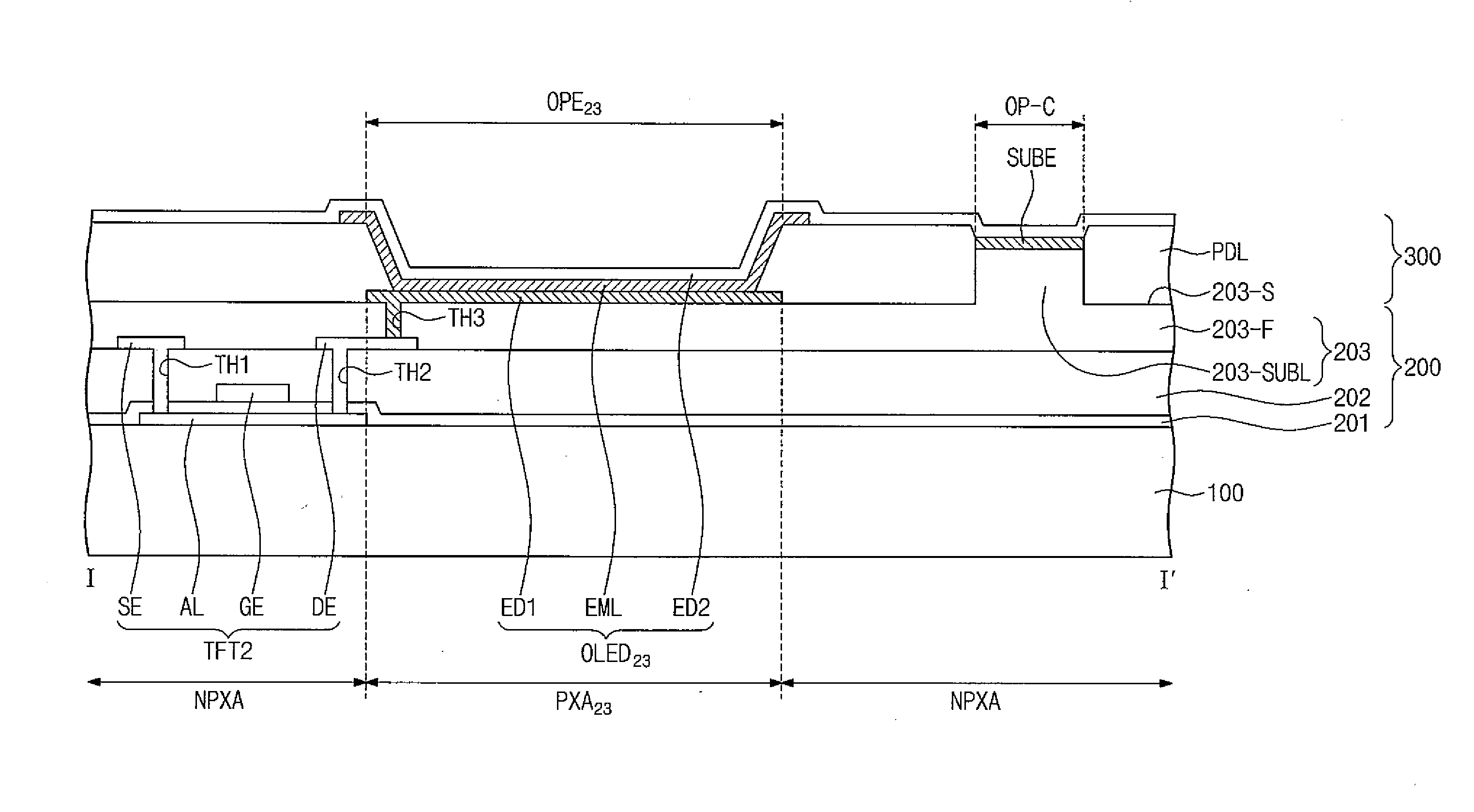
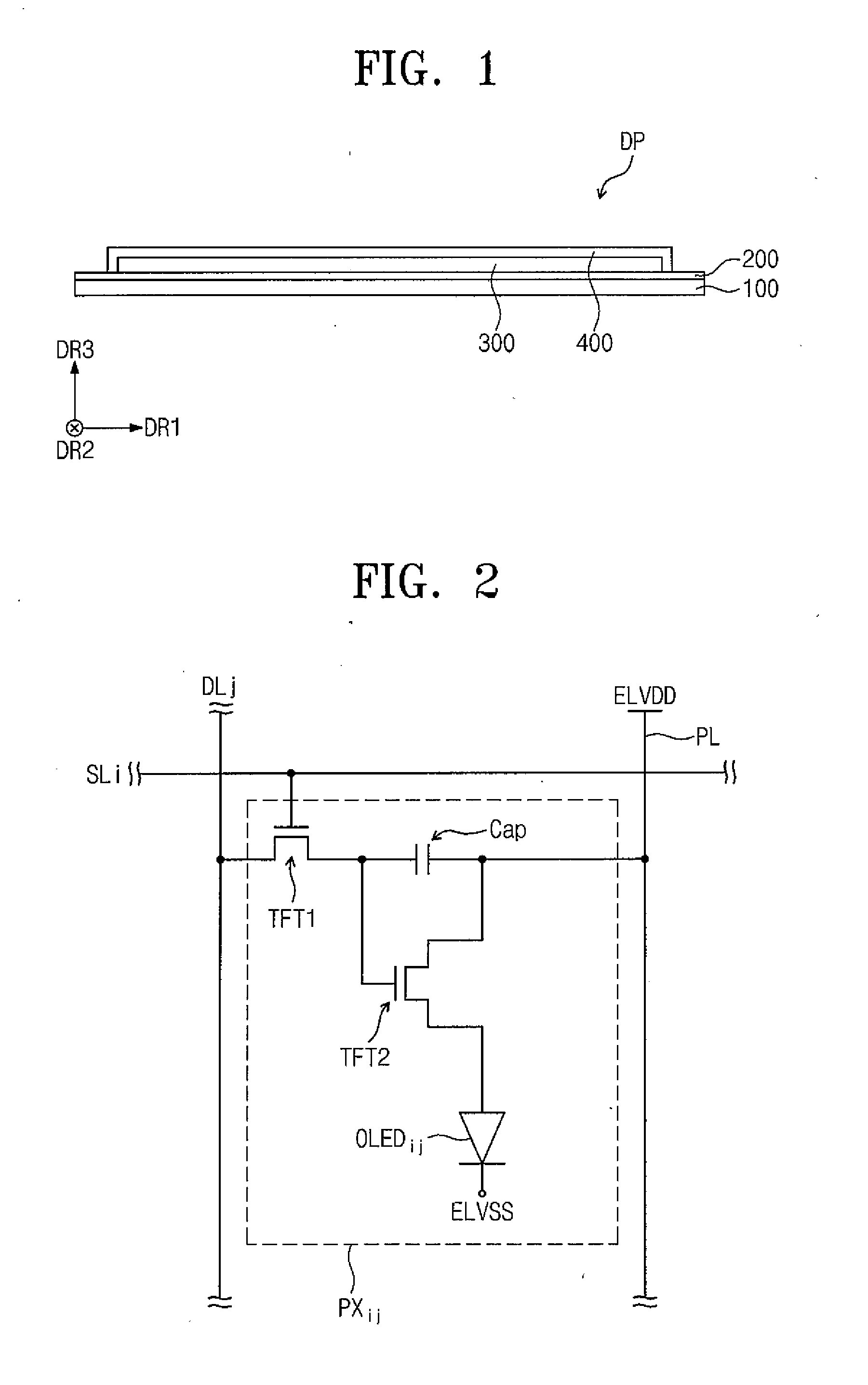
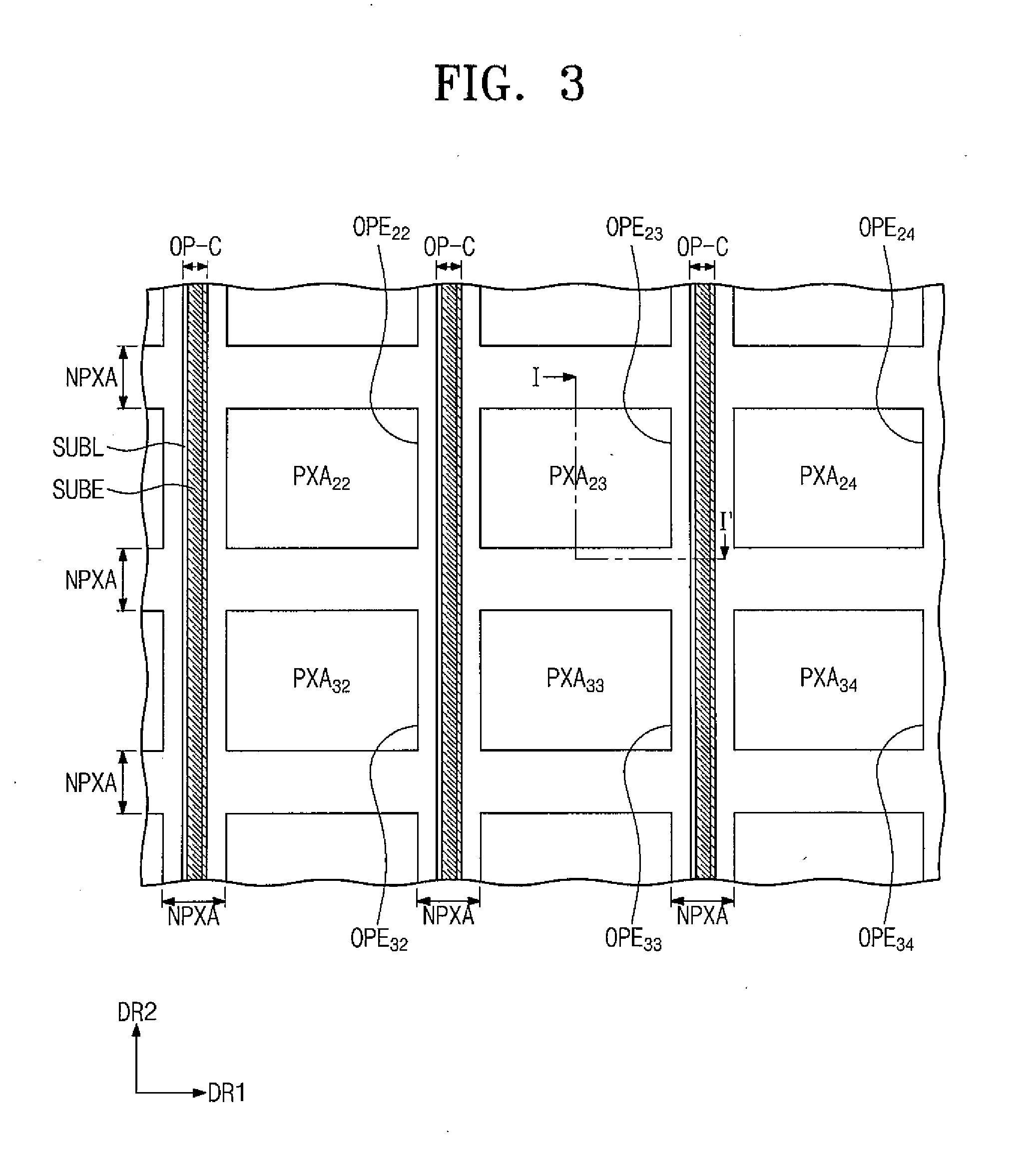
[0044]It will be understood that when an element or layer is referred to as being “on”, “connected to” or “coupled to” another element or layer, it can be directly on, connected or coupled to the other element or layer or intervening elements or layers may be present. In contrast, when an element is referred to as being “directly on,”“directly connected to” or “directly coupled to” another element or layer, there are no intervening elements or layers present. Like numbers refer to like elements throughout. As used herein, the term “and / or” includes any and all combinations of one or more of the associated listed items.

[0045]It will be understood that, although the terms first, second, etc. may be used herein to describe various elements, components, regions, layers and / or sections, these elements, components, regions, layers and / or sections should not be limited by these terms. These terms are only used to distinguish one element, component, region, layer or section from another reg...


PUM


Abstract

An organic light emitting display panel includes a base substrate; a light emitting device comprising a first electrode, a light emitting layer on the first electrode, and a second electrode on the light emitting layer; a base layer providing a base surface on which the first electrode is located; a supporting layer protruding from the base surface; a sub-electrode spaced from the first electrode, electrically connected to the second electrode, and located on the supporting layer; and a pixel definition layer on the base substrate so as to expose the first electrode and the sub-electrode.

Description

CROSS-REFERENCE TO RELATED APPLICATION[0001]This patent application claims priority to and the benefit of Korean Patent Application No. 10-2015-0007041, filed on Jan. 14, 2015, the contents of which are hereby entirely incorporated by reference.BACKGROUND[0002]1. Field[0003]The present disclosure relates to an organic light emitting display panel and a method of manufacturing the same.[0004]2. Description of the Related Art[0005]An organic light emitting display device includes a display panel including an anode electrode, a cathode electrode, and a light emitting layer disposed between the anode and cathode electrodes and including an organic material. Among display devices, the organic light emitting display device has been spotlighted as a next generation display device for its wide viewing angle and fast response time.[0006]The organic light emitting display device is classified into a front surface light-emitting type and a rear surface light-emitting type according to a transm...

Claims


Application Information

Patent Timeline
IPC IPC(8): H01L27/32H01L51/56
CPCH01L27/3246H01L51/56H01L2227/323H01L51/5221H01L51/5206H10K71/621H10K59/131H10K50/805H10K59/122H10K50/824H10K59/123H10K59/10H10K71/00H10K50/81H10K50/82H10K59/1201
Inventor LEE, SEONGMINKIM, HYOMINSHIM, CHIYEOUNG
Owner SAMSUNG DISPLAY CO LTD
Why Eureka
Try Eureka