

Determination of young's modulus of porous thin films using ultra-low load nano-indentation
a thin film, ultra-low-load technology, applied in the direction of instruments, measuring devices, investigating material hardness, etc., can solve the problems of overestimation of young's modulus by nano-indentation, virtually useless values obtained for suitability modeling purposes, and modulus, so as to reduce the modulus of the sample material
- Summary
- Abstract
- Description
- Claims
- Application Information
AI Technical Summary
Benefits of technology
Problems solved by technology
Method used
Image

Examples
Embodiment Construction
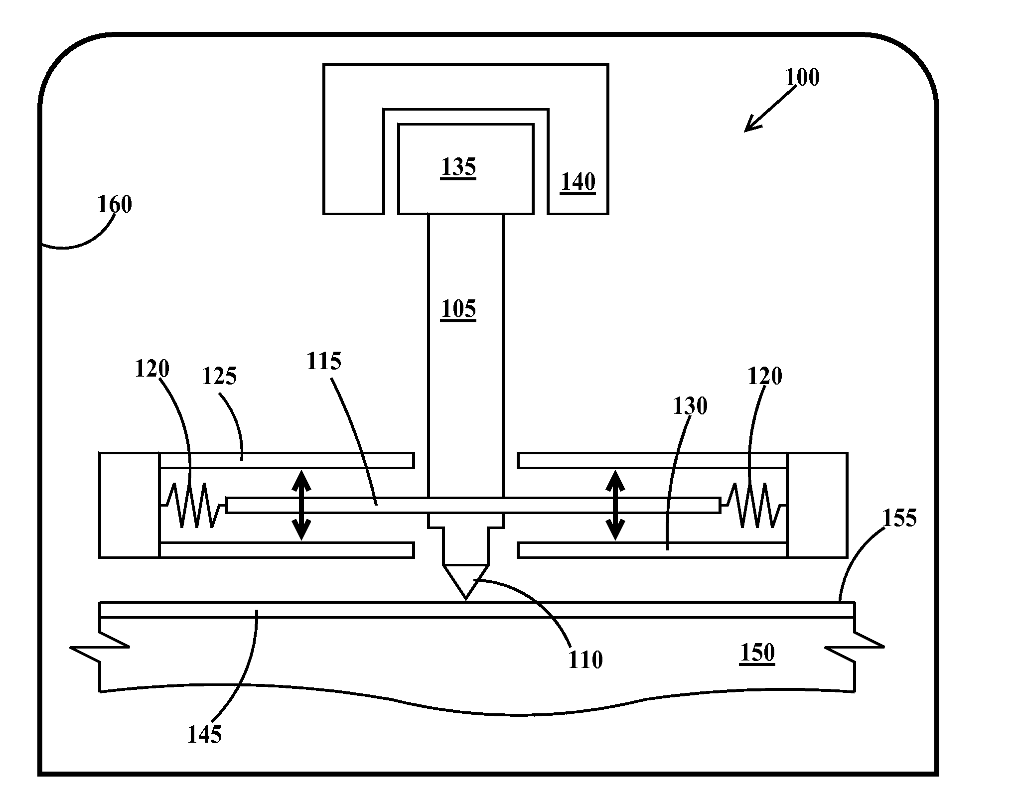
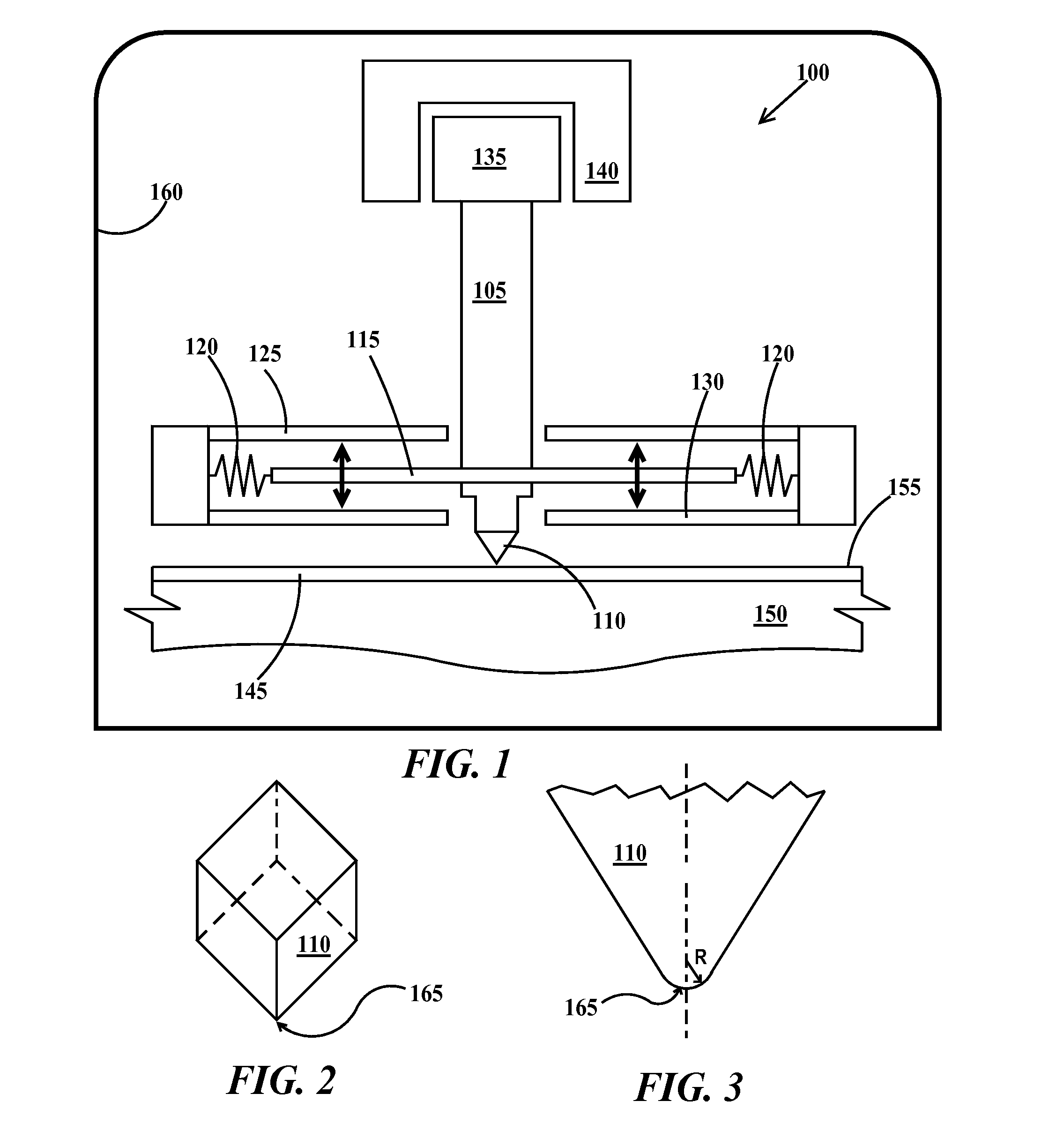
[0018]The embodiments of the present invention utilize a novel combination of ultra-low load nano-indentation and newly developed algorithms to obtain Young's modulus values for porous low-k semiconductor insulators that do not require limitation of the indentation depth and show no substrate effect.
[0019]In the miniaturization of semiconductor electronics, the metal lines that carry signals to microprocessors get ever closer, increasing parasitic capacitive losses especially when operating at frequencies in the range of hundreds of MHz. A standard in the industry today to reduce these losses is to insert between the conducting elements materials of low dielectric constant (‘low-k’), lower than silicon dioxide, which has been the insulating material of choice for almost three decades. Chemical modification of the silica network, first by the introduction of fluorine and eventually by the addition of carbon, has been adopted as a path to introducing low-k materials in manufacturing. ...
PUM
 Abstract
Description
Claims
Application Information